
This lesson demonstrates the basic features of a typical WDM optical communication system and shows the basic design steps with OptiSystem.
In this lesson we will develop a simple, realistic WDM communication system. The performance of the system will be shown and compared with published results. The impact of various physical effects accompanying the light propagation in optical fibers on the signal transmission will be analyzed. Because the analysis of a multi-channel system is useful, the natural starting point is with the analysis of a simple one-channel system.
Single-channel transmission
Figure 1 shows the layout that we use to analyze the performance of such a system. The layout is followed with detailed explanations of its components.

Figure 1: Single channel system layout
The three main blocks of each communication system shown in Figure 1 are the transmitter, the optical span, and the receiver.
Transmitter
The process of converting the digital data stream (a sequence of logical “ones” and “zeros”) into sequence of light pulses (where the presence of the pulse corresponds to “one” and the absence of a pulse corresponds to “zero”) is known as modulation. At bit rates as high as 40 Gb/s (considered here) the direct switching “on” and “off” the laser (known as direct modulation) is impossible due the transient effects taking place within the laser. Therefore, we use external modulation, which means that the laser will operate in a continuous wave mode and an external device (the modulator), will convert the data into a sequence of pulses.

Figure 2: Transmitter subsystem layout
The exact way this conversion is carried out depends on the modulation format. The global parameters of the layout shown in Figure 2 are detailed in Figure 3.

Figure 3: Global parameters
The laser is considered as ideal, so its line-width is set to zero. The phase-deviation parameter of phase modulator is set to 180°. The “10” sequence is used in the “User- defined bit sequence generator”. The modulator shown in Figure 3 has three stages. After each stage, the modulation formats known as NRZ (non-return-to-zero), RZ (return-to-zero) and CSRZ (carrier-suppressed-return-to-zero) modulation formats are produced.
The graphs produced by the time- and frequency-domain visualizers after the first, second, and third modulation stage, are shown in Figure 4, Figure 5, and Figure 6. Figure 6A shows a frequency and time domain visualization of a modulation format known as modified duobinary return-to-zero (known also as carrier suppressed duobinary return-to-zero, see [4], [29]).

Figure 4: NRZ time- and frequency-domain visualizers
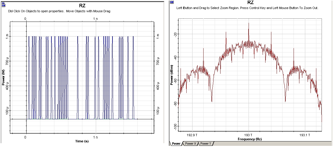
Figure 5: RZ time- and frequency-domain visualizers
Note, that the spectra of the modulation formats shown coincide with those presented in references [1],[2],[29].
We can convert each of the modulators into a subsystem, which is convenient for the further design. These subsystems are shown in Figure 7, Figure 8, Figure 9 and Figure 9.1. By varying the phase deviation parameter of the phase modulator (Figure 2) a set of formats can be produced known as alternating-phase return-to- zero [3]. At one extreme (zero phase deviation) this corresponds to the ordinary RZ, while at 180° phase deviation CSRZ will be generated.
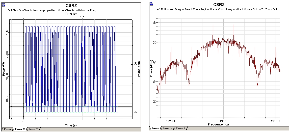
Figure 6: CSRZ time- and frequency-domain visualizers
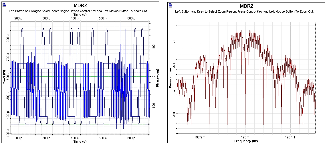
Figure 6: A MDRZ time- and frequency-domain visualizers

Figure 7: NRZ subsystem design

Figure 8: RZ subsystem design

Figure 9: CSRZ subsystem design

Figure 9.1: MDRZ subsystem design
The practical aspects of the generation of some of the most frequently used modulation formats are discussed in [2], [3], [4], [29]. The second stage (amplitude) modulator and the third stage (phase) modulator are replaced by a single dual-drive modulator with the presence (absence) of the phase modulation achieved by the appropriate biasing and alteration of the frequency of the sine generator (Bit rate/2 for 180° phase alternation and Bit rate for no phase modulation, see [2] for details). Figure 9.1 shows a design of a MDRZ modulator [4], [29].
The differences between NRZ and RZ are obvious. Additional phase modulation is introduced to RZ to convert it to APRZ/CSRZ – i.e. a phase variation between every two bits. For MDRZ this phase modulation is somewhat different. The phase of all the “zero” bits is kept constant and a 180° phase variation between all the consecutive “ones” is introduced.
Optical span
The next step is to design the transmission span (see Figure 10). The transmission span that we use consists of “cells” i.e. it is periodic. The “Loop control” component will actually perform the multiplication of our cell the necessary number of times.

Figure 10: Transmission span layout
The use of cells stems from the necessity of dispersion compensation. At bit rates as high as 40 Gb/s, the design of the cell is crucial. The dispersion length at 1.55 micrometers, assuming standard single-mode fibers (SMF), and Gaussian pulses with 0.5 duty ratio is of the order of 3 km [5], [6]. As Figure 10 shows, the period of the cell is 50 km (the length of the dispersion compensating fiber (DCF) is not included). This means that during the propagation, within one cell, not only is there a strong overlap between the adjacent pulses, but the original bit stream will be totally scrambled due to the dispersion-induced pulse broadening. This regime of propagation known as “pulse-overlapped” is of very high practical importance, since in this case the impact of the nonlinear effects taking place due to the interaction of the overlapping pulses that belong to one and same information channel (known as intra-channel nonlinearities) are reduced [7], [8]. The concept involves spreading of the pulses as far as possible and as quickly as possible in the time domain in order to create a rapidly varying intensity pattern, in order to combat the impact of the nonlinearity [12].


Figure 11: SMF parameters


Figure 12: DCF parameters
Figure 11 and Figure 12 give the parameters of SMF and DCF. They are the same as those used in [9]. The gain of the EDFA placed after each fiber is such that is compensates the losses of the preceding fiber. The noise figure of the amplifiers is constant and set to 6 dB [9]. Note that the “Model type” parameter of both fibers is set to Scalar, so no birefringence effects are considered, and consequently PMD is not taken into account.
Our first task is to analyze the performance of the single channel system depending on the dispersion cell design and input power for different modulation formats. To achieve this, we need to “sweep” a range of input power levels and, simultaneously, a range of lengths for the transmission fibers, keeping the cell length constant and equal to 50 km. This is done by using the “sweep” mode for the lengths of both transmission fibers in the cell and for the amplifier gains. The total number of iterations is set to 36. If a finer grid is needed, this number can be increased, however this will increase the total computation time. Table 1 gives an example of such a setup. The lengths of the transmission fibers (SMF and SMF_1) are chosen in such a way that the dispersion compensation scheme ranges from pre-compensation to post- compensation.
Receiver
Figure 13 shows the receiver that we use. It consists of a PIN photo-detector, fourth order low-pass Bessel electrical filter with 32 GHz (0.8 *Bit rate) cut-off frequency and a BER Analyzer with its default settings kept. The thermal noise of the photo-detector is not taken into account.

Figure 13: Receiver layout
Table 1
| EDFA Ideal 2
Gain [dB] |
SMF_1
Length [km] |
EDFA Ideal
Gain [dB] |
SMF
Length [km] |
CW Laser
Power [mW] |
| 8.33333 | 41.66667 | 1.66667 | 8.33333 | 0.5 |
| 8.33333 | 41.66667 | 1.66667 | 8.33333 | 1.2 |
| 8.33333 | 41.66667 | 1.66667 | 8.33333 | 1.9 |
| 8.33333 | 41.66667 | 1.66667 | 8.33333 | 2.6 |
| 8.33333 | 41.66667 | 1.66667 | 8.33333 | 3.3 |
| 8.33333 | 41.66667 | 1.66667 | 8.33333 | 4 |
| 6.66667 | 33.33333 | 3.33333 | 16.66667 | 0.5 |
| 6.66667 | 33.33333 | 3.33333 | 16.66667 | 1.2 |
| 6.66667 | 33.33333 | 3.33333 | 16.66667 | 1.9 |
| 6.66667 | 33.33333 | 3.33333 | 16.66667 | 2.6 |
| 6.66667 | 33.33333 | 3.33333 | 16.66667 | 3.3 |
| 6.66667 | 33.33333 | 3.33333 | 16.66667 | 4 |
| 5 | 25 | 5 | 25 | 0.5 |
| 5 | 25 | 5 | 25 | 1.2 |
| 5 | 25 | 5 | 25 | 1.9 |
| 5 | 25 | 5 | 25 | 2.6 |
| 5 | 25 | 5 | 25 | 3.3 |
| 5 | 25 | 5 | 25 | 4 |
| 3.33333 | 16.66667 | 6.66667 | 33.33333 | 0.5 |
| 3.33333 | 16.66667 | 6.66667 | 33.33333 | 1.2 |
| 3.33333 | 16.66667 | 6.66667 | 33.33333 | 1.9 |
| 3.33333 | 16.66667 | 6.66667 | 33.33333 | 2.6 |
| 3.33333 | 16.66667 | 6.66667 | 33.33333 | 3.3 |
| 3.33333 | 16.66667 | 6.66667 | 33.33333 | 4 |
| 1.66667 | 8.33333 | 8.33333 | 41.66667 | 0.5 |
| 1.66667 | 8.33333 | 8.33333 | 41.66667 | 1.2 |
| 1.66667 | 8.33333 | 8.33333 | 41.66667 | 1.9 |
| 1.66667 | 8.33333 | 8.33333 | 41.66667 | 2.6 |
| 1.66667 | 8.33333 | 8.33333 | 41.66667 | 3.3 |
| 1.66667 | 8.33333 | 8.33333 | 41.66667 | 4 |
| EDFA Ideal 2
Gain [dB] |
SMF_1
Length [km] |
EDFA Ideal
Gain [dB] |
SMF
Length [km] |
CW Laser
Power [mW] |
| 0 | 0 | 10 | 50 | 0.5 |
| 0 | 0 | 10 | 50 | 1.2 |
| 0 | 0 | 10 | 50 | 1.9 |
| 0 | 0 | 10 | 50 | 2.6 |
| 0 | 0 | 10 | 50 | 3.3 |
| 0 | 0 | 10 | 50 | 4 |
In our case, no special calibration of the receiver has been performed. The impact of the receiver calibration on the system performance estimation can be eliminated by using the eye closure penalty instead of the Q-factor as a measure of the system performance [2], [9], [10]. The receiver calibration however can be performed by sweeping the thermal noise parameter until a given value of the Q-factor (say Q=6) is achieved at a specified input power level. It should be noted however that the optimum receiver design is crucial and it is a subject of intensive research (see e.g. [23]-[27]).
Results
Using the layout shown in Figure 1, and performing the simulations, the following results are obtained for performance of the single-channel system studied (Figure 14) depending on the input power, dispersion compensation scheme and modulation format. These results are published in part in [11].
As Figure 14 shows, optimum performance is obtained with symmetric dispersion compensation. This is a well established result [12]-[15] and it does not depend on the modulation format since the intra-channel nonlinear effects depend on pulse-to-pulse interactions. A simple explanation (e.g. [15]) for this is that the nonlinear distortions accumulated in the first part of the cell are balanced by those in the second part of it.

Figure 14: Dependence of the Q-factor of a single-channel on averaged power and dispersion compensation scheme
Note: X denotes the fraction of the SMF length preceding the DCF. X=0 corresponds to precompensation, X=1 to postcompensation. Bit sequences containing 1024 bits are used.
A comparison between NRZ and RZ shows that in single channel dispersion compensated systems, RZ performs better than NRZ (see e.g. [9], [10]). The explanation is that because dispersion is compensated, RZ would perform better because it tolerates nonlinearities [10]. This situation changes however in situations where incomplete dispersion compensation is used [9] because NRZ has a narrower spectrum and therefore tolerates residual dispersion better.
The existence of an optimum input power can be explained with the interplay between the amplifier noise and the nonlinear distortions. At low power values the performance improves with the increase of power resulting from the better signal-to-noise ratio. At higher power levels however nonlinear distortions dominate [10].
The location of the maximum of the Q factor with respect to the averaged launched power shows that nonlinearity tolerance of the different formats studied is quite different. NRZ has the lowest nonlinearity tolerance. The pulse-width is not constant for NRZ which leads to different interplay between dispersion and self-phase modulation. The other reason is related to the inter-channel cross-phase modulation and four-wave-mixing. As it has been already mentioned (see [12]) the faster and further the pulse spreading occurs the smaller the impact of the intra-channel nonlinearities would be [7, 12]. This is the basic idea behind the “pulse-overlapped” transmission. Obviously, the shorter RZ pulses will spread faster which will combat the intra-channel nonlinearities better.

Figure 15: Dependence of the Q-factor of a single-channel on averaged power and dispersion compensation scheme
Note: X denotes the fraction of the SMF length preceding the DCF. X=0 corresponds to precompensation, X=1 to postcompensation. Bit sequences containing 256 bits are used.
If, however, the distortions caused by intra-channel nonlinearities depended merely on the pulse width, all RZ-based modulation formats (RZ, CSRZ and MDRZ) would perform in exactly the same way. This however is not the case. As it has been shown (see e.g. [4]) and Figure 14 shows MDRZ has a superior performance to CSRZ and RZ. This can be attributed to the fact that the spectrum of the MDRZ formats lacks discrete tones [4], which counteracts the intra-channel four-wave mixing. It has been suggested in [16] that the 180° phase inversion between the consecutive “marks” (that takes place for MDRZ) will lead to a suppression of the energy of the four-wave- mixing product that appears in a space bit (the so-called ghost pulse [14]) generated by two blocks of marks surrounding this “space”.
Figure 15 shows the results for RZ and CSRZ formats presented in Figure 14 with 256 bits Qualitatively the same results are obtained.

Figure 16: Eye closure penalty versus averaged power for different modulation formats and compensation schemes – post-compensation (a) and symmetric compensation (b). Bit stream with 256 bits is used.
Figure 15 compares the performance of all the four studied formats in terms of eye closure penalties [2], [9], [10] as a function of the launched power for the cases of post-compensation and symmetric dispersion compensation. In the case of post- compensation all the RZ-based formats show similar performance. The similar performance of RZ and CSRZ is to be expected based on the considerations of [3] and [17]. Superior performance of MDRZ has been reported earlier in [4], however different dispersion cell has been used in [4] and besides the power range covered is between 3 mW and 13 mW in [4]. With symmetric dispersion compensation scheme used the situation presented in Figure 16 (a) changes. Although all the formats improve their performance due to the suppression of the “ghost-pulses”, the improvement is different for all the formats. As Figure 16 (b) shows, the superiority of MDRZ format exists for power levels above 1 mW. Besides, for power values above 1.5 mW the difference between RZ and CSRZ becomes well pronounced. The combination of MDRZ (also called carrier-suppressed duobinary) and symmetric dispersion map has been studied experimentally for the first time in [18].
16 channels at 40 GB/s WDM transmission
This part of the tutorial discusses the design of a multi-channel WDM system. With all the blocks necessary to build a typical single channel system with OptiSystem already explained, only small modifications are needed to extend the design to multi-channel systems. The transmission span remains the same. A multiplexer must be added at the transmitter site to combine all the channels so that they can be transmitted trough the optical fibers. Respectively, a de-multiplexer must be added at the receiver site which will provide the separation of the channels in the frequency domain and they can be analyzed separately.
WDM Transmitter
One possible design of a WDM transmitter (using MDRZ modulation) is shown in Figure 17. Note that the same design can be used to transmit any desired modulation format provided that the external modulators are replaced accordingly.

Figure 17: WDM transmitter using MDRZ modulation
The parameters of the CW Laser Array component is shown in Figure 18.


Figure 18: CW Laser Array parameters
Figure 19 details the parameters of the WDM multiplexer.


Figure 19: WDM multiplexer parameters
The signal consists of 16 channels (the first one being at 193.1 THz) with 200 GHz channel spacing [9]. Although the channel spacing that we use is one and same for the channels, WDM transmission with unequal channel spacing has also been considered in the literature [19] to counteract the effect of the inter-channel FWM.

Figure 20: Expansion of signal bandwidth as a result of the inter-channel four-wave-mixing.
Note: Upper plot shows the input signal. Lower plot is the signal after 300 km transmission.1- input signal bandwidth, 2 – FWM products of interactions between the input signals (first-order), 3 – second order FWM products – result of interactions between waves that were not present at the fiber input, but are generated by nonlinear interactions between the input signals.
To ensure separation between the channels in the frequency domain (linear cross-talk suppression), before multiplexing, each channel is optically filtered with a second- order Bessel filter with a bandwidth equal to four times the Bit rate (or 160 GHz).
Although we keep the value of this parameter fixed throughout the design, it should be noted that this value depends on the modulation format used [9]. The length of the pseudo-random bit sequences used is 256 bits. Total field approach will be used to model the light propagation in the optical fiber component [5],[6] [21]. This means that the global sample rate will be such that all the sampled signals will form a single band – i.e. the simulated bandwidth (numerically equal to the sample rate) will be large enough to accommodate all the sampled signals. In our case we have 16 channels with 200 GHz channel spacing, which means that the total channel bandwidth will be 15 x 200 GHz = 3THz. Due to the inter-channel four-wave mixing (FWM) – see e.g. [19]-[21] – however the initial signal bandwidth will expand after the transmission through a nonlinear optical fiber. A typical example of this is shown in Figure 20. Recalling that the wave frequencies interacting through FWM obey f1+f2=f3+f4, it is easy to see that if only interactions between input signal frequencies are taken into account, their products will lead to a bandwidth expansion by a factor of three. These continuously generated new frequencies (known also as “spurious waves”[20]) can further interact among each other leading to further bandwidth expansion. Since only a finite bandwidth is available, it is clear that the FWM products outside the simulated bandwidth will be aliased – i.e. they will be falsely translated into the simulated bandwidth. By choosing the simulated bandwidth to be at least three times [9], [22], that of the input signal (as in our simulation) we can ensure that only “second-order” and higher FWM products (i.e. products of the products) will be aliased. As expected, (and as Figure 20 shows) their power is much smaller than that of the first order products.
To summarize, bandwidth at least three times that of the input signal must be considered if the FWM in the system is significant – which will be the case in systems with low local dispersion and/or higher input power. You should however keep in mind that the increase of the simulated bandwidth leads to an increase in the computation time.
WDM Receiver
Figure 21 shows a WDM receiver design. It consists of 1 to 16 de-multiplexer and a “single-channel” receiver (Figure 13) connected to each output port.

Figure 21: WDM receiver layout
Figure 22 shows the parameters of the WDM de-multiplexer component.

Figure 22: WDM de-multiplexer component parameters
Transmission span
Based on the results obtained in the single-channel case we are going to use symmetric dispersion compensation (Figure 23). The values of the fiber parameters (attenuation, dispersion, nonlinearities etc.) are exactly the same as in the single- channel case (see Figure 12 and Figure 13) The cell length (50km) is split to equal parts 25km each. The DCF is placed in the middle of the cell.

Figure 23: Transmission span layout
The gains of the EDFAs are such that each amplifier compensates the losses of the preceding fiber. The noise figure of the EDFAs is 6 dB. Examination of the fiber parameters (Figure 12 and Figure 13) shows that the first-order dispersion is compensated exactly (i.e. the equality DSMFLSMF=DDCFLDCF holds where D means the first-order dispersion parameter [ps/nm/km] of the corresponding fiber and L stands for the total SMF or DCF length per cell). The second-order dispersion (dispersion slope) is not compensated exactly, which means that in total dispersion, compensation takes place only at a certain wavelength. This is the carrier wavelength, which (since it is not explicitly specified in the set-up) is assumed by the fiber components to correspond to the center frequency of the simulated bandwidth. Due to the incomplete dispersion compensation, the longest-wavelength channel accumulates approximately 9 ps/nm (positive) dispersion per single cell. The shortest wavelength channel accumulates -9 ps/nm dispersion per cell. One of our tasks is to identify how the interplay between this residual dispersion and the nonlinearity (SPM) influences the performance of the system depending on the modulation format.
Variable step-size is used with the maximum (over the time window) nonlinear phase shift allowed equal to five mrad. This is consistent with what is used in the literature (e.g. one mrad is used in [9] and three mrad in [21]). In the presence of loss, the impact of the nonlinearities will decrease along the fiber length (or more specifically, the nonlinearities will be important until the propagation distance is less than the effective length [5]) which subsequently allows larger step-sizes to be used – the variable step size calculation is advantageous in this case. It is well established that if the step size is improperly chosen (too big), the FWM effects will be artificially exaggerated [28]. Boundary conditions must be set to periodic.
Results
Figure 24 shows the dependence of the Q-factor of the system on the channel power and channel number (that is, the amount of the residual dispersion).
The largest area with best performance, i.e. the largest number of channels and largest region of powers with maximum Q, is obtained for MDRZ. The CSRZ has the second best performance. This observation is consistent with results from the single channel analysis, in accordance with the very basic idea that the intra-channel nonlinear interactions are more important than the inter-channel one.
 and averaged channel power.")
Figure 24: Q-factor of a 16 x 40 Gb/s WDM system depending on the channel number (i.e. the amount of residual dispersion) and averaged channel power.
Note: Symmetric compensation scheme is used. Channel number one is the longest wavelength channel.
As Figure 24 shows, there is a noticeable asymmetry in the performance of NRZ. With the increase of the channel power, the outer channels with longer wavelengths (with numbers from 1 to 4) improve their performance with the power increase, while the performance of the shorter-wavelength channels (with numbers from 12 to 16) degrades. This feature can be attributed to the interplay between the residual dispersion and nonlinearity. As already mentioned, the longest-wavelength channel (channel number 1) accumulates approximately 9 ps/nm positive dispersion per single cell. The resulting negative chirp tends to compensate the positive one created by nonlinearity, with the degree of compensation increasing with the increase of power, which explains the observed improvement in performance. On the other hand, the residual dispersion is negative for the shorter-wavelength channels, and the effects of residual dispersion and nonlinearity are added together, which degrades the performance of these channels with the power increase.
In a weaker form, this effect could also be seen for the RZ. At the same time, MDRZ and CSRZ demonstrate almost complete symmetry in the performance of the outer channels. The smaller resistance of NRZ compared to RZ to the interplay between dispersion and nonlinearity is a well established fact (see e.g. [10]).
References:
[1] D. Dahan and G. Eisenstein, Journ. Lightwave. Technol. 20, 379 (2002).
[2] A. Hodzik, B. Konrad and K. Petemann, Journ. Lightwave. Technol. 20, 598, (2002).
[3] P. Johannison, D. Anderson, M. Marklund, A. Berntson, M. Forzati and J. Martensson, Opt. Lett.
27, 1073, (2002).
[4] K.S. Cheng and J. Conradi, IEEE Phot. Technol. Lett., 14p. 98, (2002).
[5] G. P. Agrawal, Nonlinear Fiber Optics, Academic press (2001).
[6] G. P. Agrawal, Applications of Nonlinear Fiber Optics, Academic press (2001).
[7] P.V. Mamyshev and N.A. Mamysheva, Opt. Lett. 24, 1454, (1999).
[8] A. Mecozzi, C.B. Clausen, M. Schtaif, IEEE Phot. Technol. Lett., 12, 392 (2000).
[9] M.I. Hayee and A.E. Willner, IEEE Phot. Technol. Letters, 11, 991, (1999).
[10] D. Breuer and K. Petermann, IEEE Phot. Technol. Lett. 9, 398, (1997).
[11] K. Marinov, I. Uzunov, M. Freitas and J. Klein, Optical amplifiers and their applications (OSA Topical meeting), 76 – 78, Otaru, Japan, July 6 – 9 (2003).
[12] A. Mecozzi, C.B. Clausen, M. Schtaif, IEEE Phot. Technol. Lett., 12, 1633, (2000).
[13] A. Mecozzi, C.B. Clausen, M. Shtaif, IEEE Phot. Technol. Lett., 13, 445 (2001).
[14] P. Johannisson, D. Anderson, A. Bernutson and J. Martensson, Opt. Lett., 26, 1227, (2001).
[15] R. I. Killey, H. J. Thiele, V. Mikhailov and P. Bayvel, IEEE Phot. Technol. Lett., 12, 1624, (2000).
[16] X. Liu, X. Wei, A. H. Gnauck, C. Xu and L. K. Wickham, Opt. Lett. 27, 1177, (2002).
[17] Forzati, and J. Martensson, A. Bernutson, A. Djupsjobaska, P. Johannisson, IEEE Phot.
Technol. Lett., 14, 1285, (2002).
[18] Y. Miyamoto, A. Hirano, S. Kuwahara, Y. Tada, H. Masuda, S. Aozasa, K. Murata, and H.
Miyazawa, Technical Digest of OAA 2001, post-deadline paper PD6, July, (2001).
[19] F. Forghieri, R. W. Tkach and A. R. Chraplyvy, Journ. Lightwave. Technol., 13, 889, (1995).
[20] D. Marcuse, A. R. Chraplyvy and R. W. Tkach, Journ. Lightwave. Technol, 9, 121, (1991).
[21] R. W. Tkach, A. R. Chraplyvy, F. Forghieri, A. H. Gnauck, and R. M. Derosier, Journ. Lightwave.
Technol, 13, 841, (1995).
[22] F. Matera and M. Settembre, Journ. Lightwave. Technol., 14, 1, (1996).
[23] L. Boivin and J. Pendock, Optical amplifiers and their applications, 292, (1999).
[24] P. Winzer, M. Pfennigbauer, M. Strasser and W. Leeb, Journ. Lightwave Technol. 19, 1263, (2001).
[25] P. Winzer and A. Kalmar, Journ. Lightwave Technol., 17, 171, (1999).
[26] M. Pauer, P. Winzer and W. Leeb, Journ. Lightwave. Technol. 9, 1255, (2001).
[27] C. H. Kim, H. Kim, P. J. Winzer and R. Jopson, IEEE Phot. Technol. Lett. 14, 1629, (2002).
[28] O. Sinkin, R. Holzlohner, J. Zweck and C. R. Menyuk, Journ Lightwave Technol. 21, 61 (2003).
[29] Y. Miyamoto, K. Yonenaga, A. Hirano and M. Tomizawa, IEICE Trans. Commun., E85-B, 374, (2002).