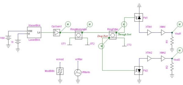
In this tutorial, we demonstrate a ring switch that adds or drops channels by controlling the index of a ring resonator.
Sample: RingSwitch.osch
Figure 1: Schematics of Ring Switch
The ‘LaserBlck’ is a subcircuit block that contains a circuit for driving laser diode. The laser diode is also connected with a thermal network consisting of thermal resistance and capacitance so that it models the temperature dependence effects. Figure 2 shows the ‘LaserBlck’ subcircuit where the thermal network wiring is drawn in red.
Figure 2: LaserBlck Subcircuit
The laser is driven by a DC voltage source ‘Vi’ so that the laser output is CW with the wavelength of 1558 nm. It is amplified by the optical amplifier ‘OptGain1’ and then modulated by a ring resonator ‘RingModulator’. RingModulator has voltage controlled index which is controlled by a small negative voltage (peak negative -0.15 mV) by the node ‘vcmod’. The node ‘vcmod’ is connected at the negative terminal of the bit generator ‘ModBitIn’. When the controlling voltage reaches a certain negative value (when logic 1), the RingModulator transmits it through the through port and at other times (logic 0) it drops the channel. As a result it behaves as a modulator to modulate the optical power according to the bit sequence input.
The modulated output is connected to the second ring resonator, ‘RingFilter’. Index of Ringfilter is controlled by the voltage at the node ‘vcfilter’ set by a piece-wise-linear voltage source ‘VfilterIn’. The transient voltage waveform by the source VfilterIn is given by Figure 3.
Figure 3: Voltage of the source VfilterIn
When the voltage source is at -900 μV (from 0 to 3.5 ns), RingFilter is set to transmit the channel to the through port. During the transition period (3.5 ns to 6.5 ns) the amplitude at the through port will be decreasing. The drop port will have the opposite effect; at -900 μV the output amplitude will be very low and will be increasing during transition period. At 6.5 ns when it reaches -100 μV, the amplitude at the through port will be very low, while the channel will be transmitted through the drop port.
Optical outputs from through port and drop port are connected to photodiodes Pd1 and Pd2 respectively. Photodiodes are connected to electrical amplifiers and output voltages are obtained at nodes Vout1 and Vout2.
Analysis:
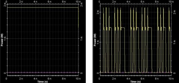
Transient analysis for this circuit is performed for 10 ns time period.Figure 4 shows optical power after OptGain1 and the Ringmodulator output. Figure 5 shows the output at through port and drop port respectively. Figure 6 shows voltages at Vout1 and Vout2.
From the graphs you can clearly observe the phenomenon of adding and dropping of channel according to the RingFilter control voltage given by Figure 3.
Figure 4: Optical power outut at OptGain1 and RingModulator
Figure 5: Optical power output at throgh port and drop port of RingFilter
Figure 6: Voltages at Vout1 and Vout2


