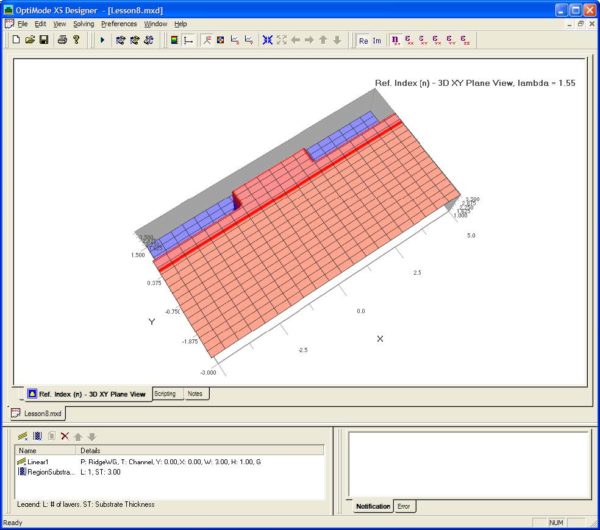
The EtchedFilmThickness will be used to define the thickness of the substrate layer.
To add the substrate layer to the layout, follow these steps:
| Step | Action |
| 1 | Click on the Add Substrate layers button, next to the Waveguide button of Figure 5. Double click on the new item in the list to get the Substrate Region dialog box |
| 2 | Click Add to get the Layers dialog box, and enter EtchedFilmThickness for the Thickness. |
| 3 | Set the material to Film from the combo box. |
| 4 | leave both dialog boxes by Clicking OK.
The refractive index view will now show the film of thickness 0.4 microns covering all the substrate. |
Figure 6: Ridge Waveguide
Note that the Substrate Layer is available in OptiBPM as well. Use this feature for designing ridge waveguides or other waveguides that have a multilayer film on the wafer between waveguides. The Layout in OptiBPM Designer will show the location of the ridges, and is the appropriate picture for preparing the layout masks.


