The objective of this lesson is to demonstrate the ability to modulate optical signals in formats different of the common RZ and NRZ.
In this tutorial our goal is to generate a 40 Gb/s optical signal in the proposed modulation formats:
- duobinary
- modified-duobinary (MDRZ)
- Carrier-suppressed RZ (CSRZ), DPSK and DQPSK formats
To generate the optical signals we have used a CW laser source, Mach-Zehnder modulators, NRZ pulse pattern generator and a sinusoidal electrical signal generator.
Furthermore, we have used a duobinary precoder for the duobinary and MDRZ signals in order to avoid recursive decoding in the receiver.
Figure 1 shows a system transmitting a Duobinary signal at 40 Gb/s (sample Duobinary_Signal.osd).
The Duobinary was generated by first creating an NRZ doubinary signal using a precoder and a duobinary pulse generator. The generator drives the first MZM, and then concatenates this modulator with an second modulator that is driven by a sinusoidal electrical signal with the frequency of 40 GHz.
The duobinary precoder used here was composed of an exclusive-or gate with a delayed feedback path.
Figure 1: Duobinary system layout
The optical signal at the output of the second MZ modulator is shown in Figure 2.
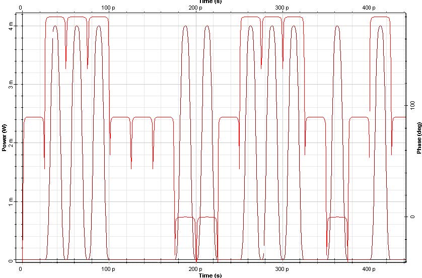
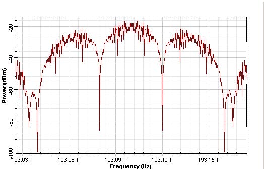
Figure 2: Duobinary signal (b) spectra
The CSRZ signal is generated in a similar way to the RZ format. However, the frequency of the sinusoidal electrical signal applied in the second MZM has half of the bit rate, 20 GHz.
The second MZM was biased in a way to provide alternating optical phases between 0 to π for the neighboring time slots.
Figure 3 shows a system transmitting a CSRZ signal at 40 Gb/s (sample CSRZ_Signal.osd).
Figure 3: Carrier-suppressed RZ system layout
The CS-RZ optical signal is shown in Figure 4.
We can see in Figure 4(a) that the phase of bits ‘1’s are alternating with a difference of π (180o). This phase difference causes the elimination of the carrier at 193.1THz.
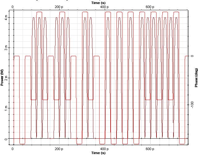
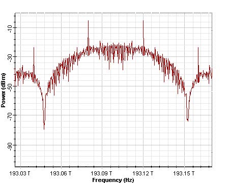
Figure 4: CSRZ signal (a) Time domain, and (b) spectra
The MDRZ was generated by first creating an NRZ doubinary signal using an delay-and-subtract circuit that drives the first MZM [1], and then concatenating this modulator with a second modulator that is driven by a sinusoidal electrical signal with the frequency of 40 GHz.
The duobinary precoder used here was composed of an exclusive-or gate with a delayed feedback path.
Figure 5 shows a system transmitting a MDRZ signal at 40 Gb/s (sample MDRZ_Signal.osd).
Figure 5: Modified duobinary RZ system layout
The MDRZ signal is shown in Figure 6.
Different of the duobinary signal where the phase of bits ‘1’s are modified only after a bit ‘0’ appear, in the modified duobinary signal the phase is alternated between 0 and π for the bits ‘1’.
This will cause the difference in the signal spectra shown at Figure 6(b).
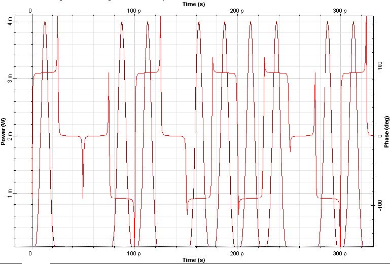
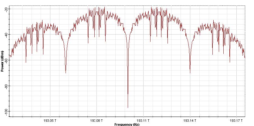
Figure 6: MDRZ signal (a) Time domain (b) spectra
For the DPSK signal generation, we continue to use two concatenated modulators.
The phase modulation was generated by first encoding the NRZ signal using a duobinary precoder that drives the first MZM and modulates the phase of the CW signal, and then concatenating this modulator with an second modulator driven by a sinusoidal electrical signal with the frequency of 20 GHz.
The encoding in the initial bit sequence will allow the demodulation of the transmitted signal at the receiver by using a Mach-Zehnder interferometer and balanced photodiodes.
Figure 7 shows a system transmitting a DPSK RZ with 33% of duty-ratio signal at 40 Gb/s (sample DPSK_33%_Signal.osd).
Figure 7: DPSK RZ 33% system layout
The DPSK signal is shown in Figure. 8.
We can verify a sequence of bit ‘1’ with the information modulated in the phase of if bit ‘1’ (0, p).
The corresponding signal spectrum is shown at Figure 8(b).
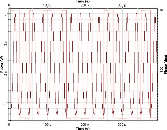
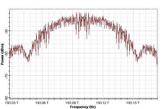
Figure 8: DPSK 33% RZ signal (a) Time domain, and (b) spectra
The generation of a DPSK signal with 66% of RZ duty-ratio is very similar to the system in the last layout. Only the phase and amplitude in sinusoidal electrical signal and the bias voltage in the second MZM are modified to generate the RZ signal with 66% of the duty-ratio.
The new layout can be seen in Figure 9 (sample DPSK_33%_Signal.osd).
Figure 9: DPSK RZ 66% system layout
The DPSK signal is shown in Figure. 10.
We can verify a sequence of bits ‘1’ with the information modulated in its phase.
The correspondent signal spectrum is shown at Figure 10(b).
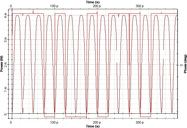
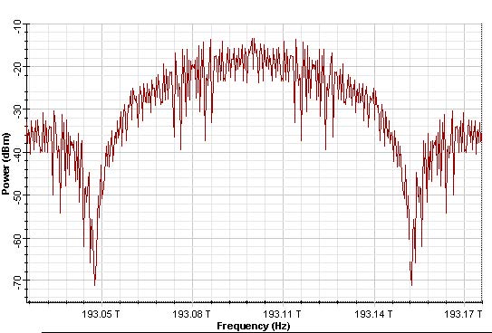
Figure 10: DPSK 66% RZ signal (a) Time domain, and (b) spectra
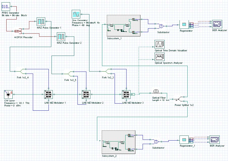
Finally, using three MZ modulators concatenated can generate the DQPSK signal format.
However, to do that, the information has to be encoded in way to allow the demodulation in the reception using two set of interferometers and balanced receivers.
The codification in the initial information was done using the DPSK component (precoder) that will simulate a precoder and generate two encoded signals that will modulate the first and second MZ modulator.
The last modulator will generate the RZ signal.
Figure 11 shows the DQPSK layout (see sample DQPSK_Signal_33%.osd).
Figure 11: DQPSK system layout
Each transmitted symbol conveys two bits, encoded in four possible phase differences between successive symbols as can be seen in Figure 12(a).
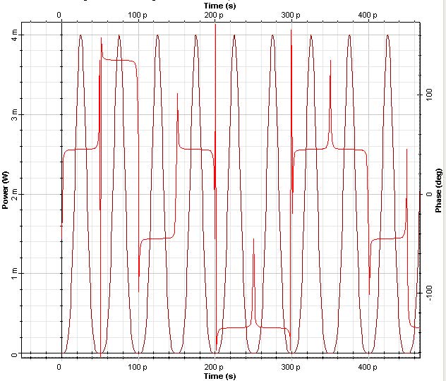
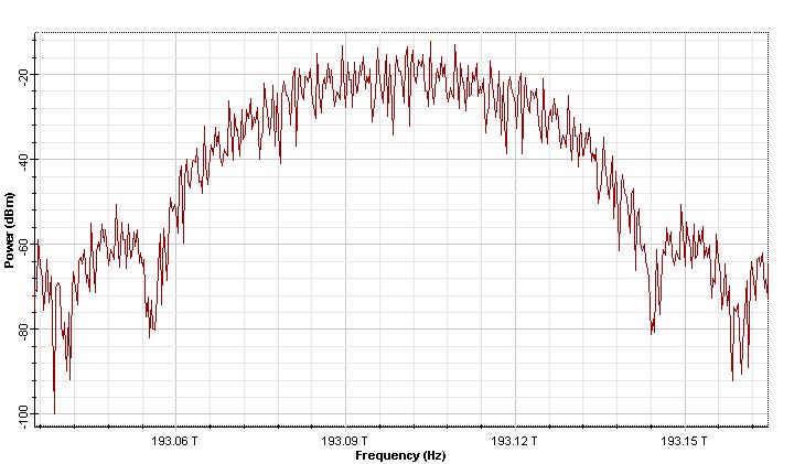
Figure 12: DQPSK signal (a) Time domain, and (b) spectrum
References:
[1] Y. Miyamoto, K. Yonenaga, A. Hirano and M. Tomizawa “Nx40 – Gbit/s DWDM transport system using novel return-to-zero formats with modulation bandwidth reduction”, IEICE Transaction Communications, vol. E85-B, 374-385, (2002).


