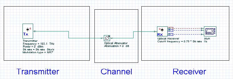
FOCS Introduction Lightwave System Components.osd details a generic block diagram of an optical communication system.
An optical communication system consists of a:
•transmitter
•communication channel
•receiver (see Figure 1)
Figure 1: Lightwave System Components
Optical transmitter
The role of the optical transmitter is to:
•convert the electrical signal into optical form, and
•launch the resulting optical signal into the optical fiber.
The optical transmitter consists of the following components:
•optical source
•electrical pulse generator
•optical modulator (see Figure 2).
The launched power is an important design parameter, as indicates how much fiber loss can be tolerated. It is often expressed in units of dBm with 1 mW as the reference level.
Fiber loss is, of course, an important design issue, as it dictates the repeater spacing of a long- haul lightwave system. Another important design issue is fiber dispersion, which leads to broadening of individual pulses inside the fiber.
In order to observe the effects of loss and dispersion in the optical signal, you can change the values of fiber length and visualize the degradation of the signal at the receiver stage.
Figure 3: Fiber 60 km
Optical receivers
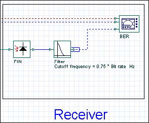
An optical receiver converts the optical signal received at the output end of the optical fiber back into the original electrical signal.
The receiver consists of the following components:
•photodetector
•filter
•demodulator (see Figure 1)
Figure 1: Receiver components
Often the received signal is in the form of optical pulses representing 1 and 0 bits, and is converted directly into an electrical current. Such a scheme is referred to as intensity modulation with direct detection (IM/DD). Demodulation is achieved by a decision circuit that identifies bits as 1 or 0, depending on the amplitude of the electrical current.
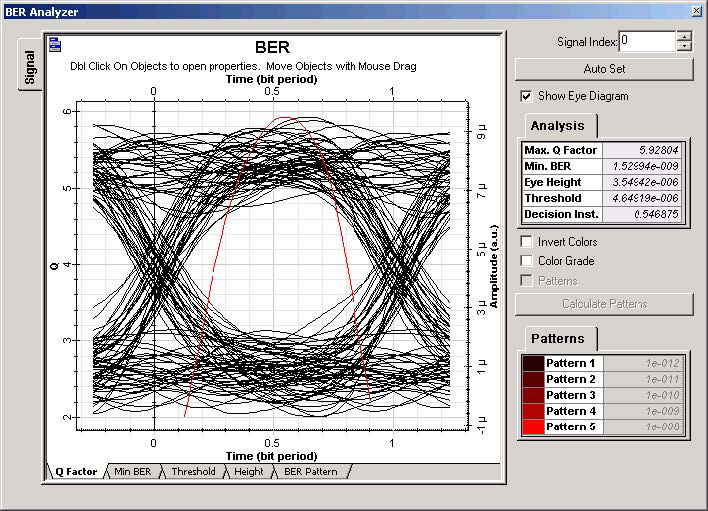
The performance of a digital lightwave system is characterized through the bit-error rate (BER). It is customary to define the BER as the average probability of incorrect bit identification. Most lightwave systems specify a BER of 10-9 as the operating requirement.
In the sample BER Analyzer diagram shown in Figure 2, a laser output power of 0 dBm and 105 km of fiber length will have a BER close to 10-9.
The design of an optical receiver depends largely on the modulation format used by the transmitter. Receiver Design.osd details a digital receiver whose components can be arranged into three groups:
•front end
•linear channel
•data-recovery
Figure 3: Receiver Design
The front-end of a receiver consists of a photodiode with a built-in preamplifier. The linear channel consists of a high-gain amplifier and an low-pass filter. The data recovery is done by the BER Analyzer with a built-in clock recovery and decision circuit.
The linear channel has a low pass filter that shapes the pulse. The receiver noise is proportional to the receiver bandwidth and can be reduced by using a low-pass filter whose bandwidth is smaller than the bit rate. The pulse spreads beyond the time slot – the spreading can interfere with the detection of neighboring bits, which is the phenomenon referred to as intersymbol interference (ISI).
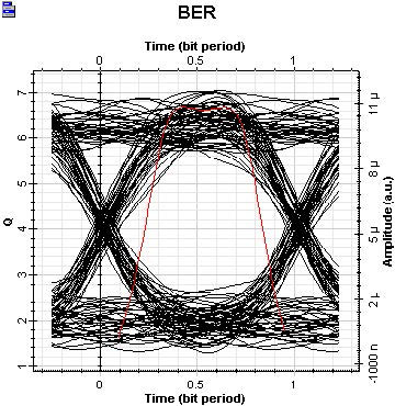
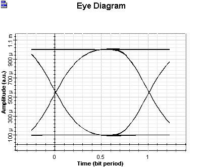
When you set the attenuation to 0 dB, the ideal eye diagram seen in Figure 4 is generated.
Figure 4: Receiver EYE Ideal
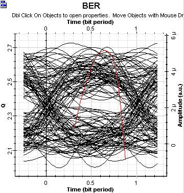
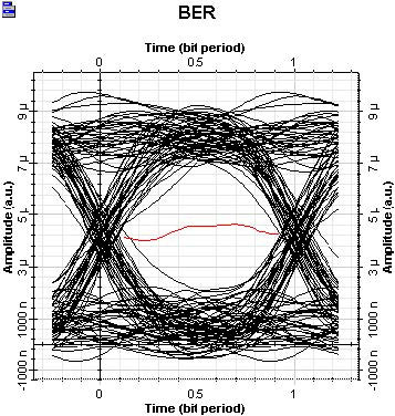
If you set the attenuation to 21 dB, the degraded eye diagram seen in Figure 5 is generated.
Figure 5: Receiver EYE Degraded
The decision circuit compares the output from the linear channel to a threshold, at a decision instant determined by the clock recovery circuit, and decides whether the signal corresponds to bit 1 or bit 0. The optimum threshold level is calculated for each decision instant in order to minimize the BER (see Figure 6).
Figure 6: Receiver EYE Threshold


