
OptiSPICE 5.0 introduces new electrical models for characterizing hetero-structure bipolar transistors (Mextram and Agilent), a physical model for spiral inductors (for Si and III-V based substrates), and a new Waveguide Crossing device.
New Features in OptiSPICE 5.0
0.00 KB
New HBT Models for BJTs
Further to the Integral charge control model of Gummel and Poon, new models have been added to the bipolar junction transistor (BJT) model, including the Mextram 504 model [1] for Si/SiGe devices and the Agilent HBT model [2] for III-V based materials.
Designers will now be able to accurately characterize the performance of HBT-based, high speed (>10 GB/s) BJT configurations for laser and modulator current drivers and receiver amplifier designs.
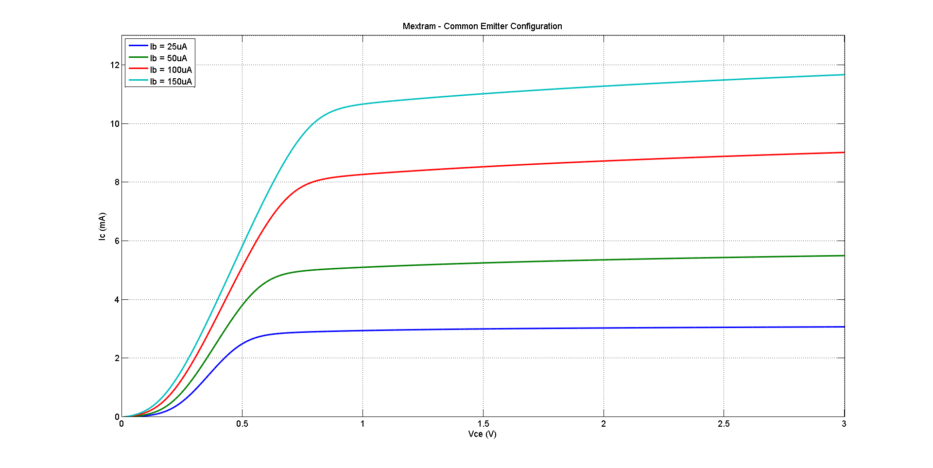
Fig 1: Example sweep plots (Ic as a function of Vce for different base currents) for the Mextram common emitter configuration.
For the Mextram 504 model in a BJT simulation (with model name “mextram”), use the following (for NPN and PNP BJT configurations):
.model mextram NPN level = 504 <param1=val1> <param2=val2>…
.model mextram PNP level = 504 <param1=val1> <param2=val2>…
For the Agilent HBT model in a BJT simulation (with model name “agilent”), use the following (for NPN and PNP BJT configurations):
.model agilent NPN level = 101 <param1=val1> <param2=val2>…
.model agilent PNP level = 101 <param1=val1> <param2=val2>…
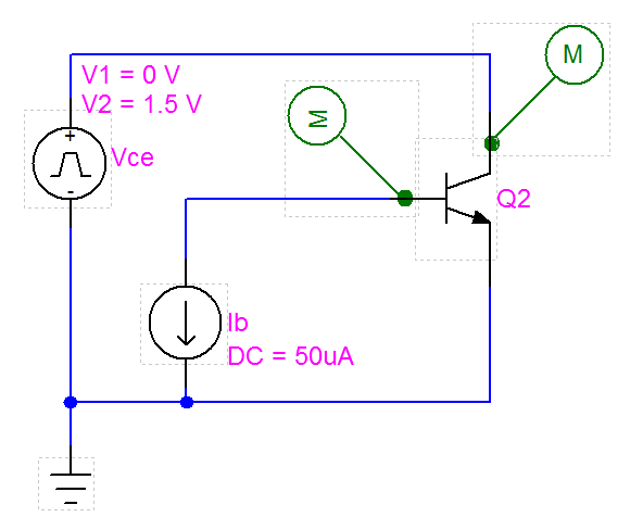
Fig 2: BJT (Mextram) Common Emitter configuration.
New Physical Model for Spiral Inductors
A new physically-based inductor model is now available for the Inductor element. The Inductor Model utilizes a lumped circuit approach (Fig 3) to model the electrical characteristics of a spiral inductor[3]. Mathematical methods for calculating the inductance (Ls) of square, hexagonal, octagonal, and circular planar inductors are also included. These methods include the Modified Wheeler, Current Sheet and Monomial expressions.
The Inductor model works for both Si and III-V based substrates.
Example Netlist format
An Inductor L1 with model name “SiInductorModel” and a line-width of 29.7e-6, is defined as follows:
L1 1 0 SiInductorModel
.model SiInductorModel IntInd w = 29.7e-6
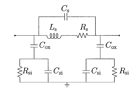
Fig 3: OptiSPICE 5.0 Lumped Circuit model for Spiral Inductors.
New Waveguide Crossing Device
The Waveguide Crossing device simulates the transmission and reflection effects that occur when two waveguides cross. This new device is useful for the design and performance analysis of integrated photonics circuits for on-chip optical interconnect and switches (such as micro-ring based routing elements).
The waveguide crossing device is based on the XCOUPLER model (the ElemType must be set to WGUIDECROSS to enable the model for this type of application).
Example Netlist format
For a waveguide with device name WC1 connected to signals SIG1, SIG2, SIG3 and SIG4 and with a through port transmission of = 0.7, a right port transmission of 0.1, a left port transmission of 0.1 and a return reflection of 0.1, the Netlist statement to be generated as follows:
Osp XCOUPLER Name=WC1 Nodes= [SIG1 SIG2 SIG3 SIG4] MoName=WC_MODEL
+ Through=0.7 Right=0.1 Left=0.1 Ref=0.1
Osp Model Name = WC_MODEL type = XCOUPLER ElemType=WGUIDECROSS
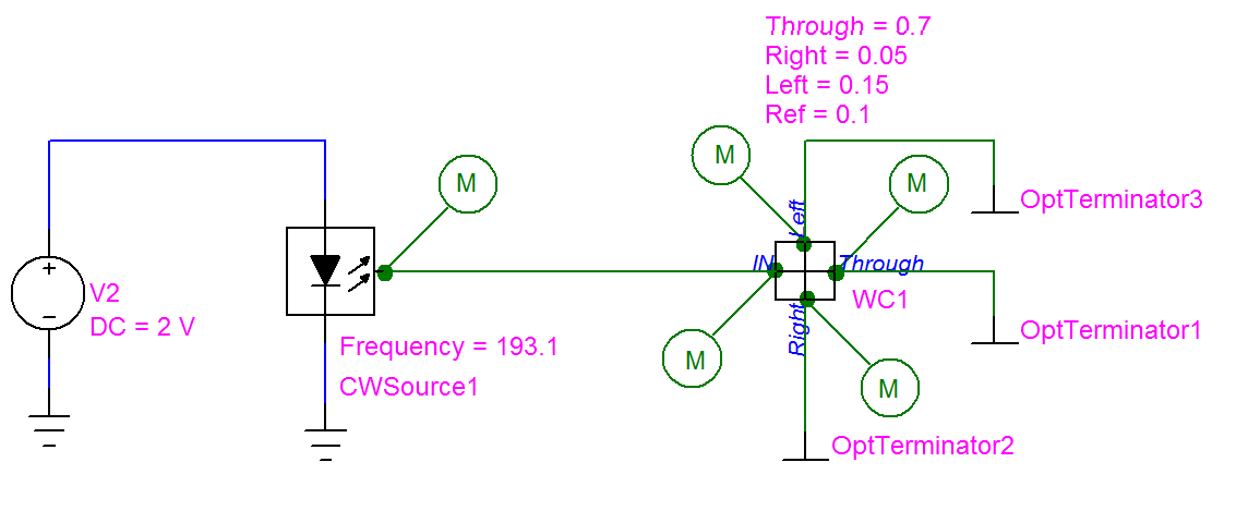
Fig 4: New waveguide crossing component.
[1] NXP Mextram
[3] S.S. Mohan, M.M Hershenson, S.P. Boyd, and T.H. Lee, Simple Accurate Expressions for Planar Spiral Inductances, IEEE Journal of Solid-State Circuits, Vol. 34, No. 10, October 1999
New Features in OptiSPICE 5.0
0.00 KB