1.1 Setting and Simulating Supercell
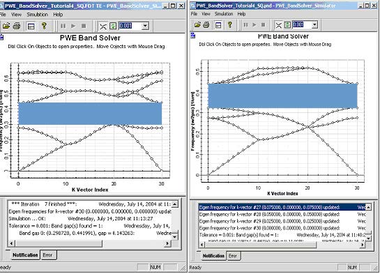
The rectangular lattice of dielectric rods with permittivity 8.9 suspended in air was investigated earlier in Lesson 2—Input wave setup. We found that the TE solutions (Optiwave convention) exhibit a band gap in the range between 0.324 and 0.442. First we have a look what is going to happen if we increase the simulation domain so that it contains several unit cells. Change the supercell definition to (#a,#b,#c)=(1,1,2) and mesh to 16x16x32. Run a TE simulation again. Notice that the band diagram looks very much different than in the case of 1x1x1 supercell (See Figure 1a). A band gap can be still located but this time it is wider and spans from 0.291 to 0.442. Change the supercell again to (2,1,2) and mesh to 32x16x32 and run simulation again. This time the band structure is again totally different (See Figure 1b). Nevertheless, the band gap in the last simulation is correct. The important fact to notice is so called folding of the bands. For (1,2) supercell there are two bands below the band gap, and in case of (2,2) supercell there are four bands. This is due to the fact that the new domain contains 2 and 4 elementary unit cell within the supercell.
Figure 1: Band diagram of a supercell 1×2 (left) and supercell 2×2 (right) for k-path selected along the irreducible Brillouin’s zone for square lattice (‘SquareZX’: G-X-M-G).
By creating a (1,2) supercell we broke up the 4-fold symmetry of the original square cell and what used to be an irreducible Brillouin zone in case of square lattice is only a part of a new irreducible zone in case of rectangular supercell. To get a correct band gap we need to scan along the edges of the irreducible Brillouin zone. Add two new major k-points to the k-path:
X2=(0.5, 0.0, 0.0) 10 divisions
M =(0.5, 0.0, 0.5) 10 divisions
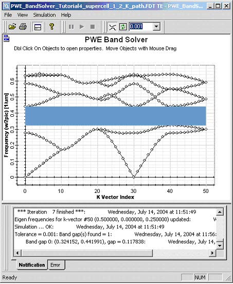
Run the simulation for (1,2) supercell. You will again observe the band folding and this time you will get correct band gap in agreement with our original simulation.
Figure 2: Band diagram of the supercell 1×2 for k-path along the edges of irreducible Brillouin’s zone for rectangular lattice (G-X-M-G-X2-M)
1.2 Setting up a defect
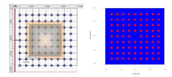
Changing the size or refractive index of a selected atom on the lattice can create a defect in the lattice. We will investigate a defect created by a missing dielectric rod. First please set the cell number to 9X9 on the original layout, then we need to remove the element from the lattice. Select the lattice in the layout, the ‘PBG Crystal Structure Cell Editing Tool becomes highlighted in the Tools toolbar. Select it, then right click on the unit cell (5,5) and select Cells Off. The cylinder in the center of the lattice will be turned off. You can check this in 2D refractive index view (see Figure 3).
Figure 3: Layout (left) and refractive index (right) of a square lattice with missing dielectric rod (defect). Supercells 5×5 and 6×6 are shown with domain origins.
What is going to happen if we run a simulation on a supercell domain with the defect?
If there is a localized defect mode confined close to the defect we should see a
straight band within the band gap of the unperturbed square lattice, i.e. in the interval
(0.324, 0.442). If the simulation domain is small and the localized mode extends to
the simulation boundaries there is coupling between the adjacent defect on the
supercell lattice and its result will be a defect band within the original band gap. Thus
when simulation defects we need to insure that the simulation domain is large enough
so that the localized band if it exist is narrow within our tolerance. The following
simulation of the whole k-path is often not necessary to study point defects. A single
k-vector simulation will usually suffice. It is however illustrative. We will perform
simulation on a supercell 5×5 so that we can observe the localized state. We have
already created the defect on the layout. Now we have to set the simulation Domain
Origin. In the figure above you can see two rectangular regions marked by different
colors. The inner region defines a suitable 5×5 supercell, the outer rectangle 6×6
supercell. Notice that a supercell selected in such manner possesses an inversion
symmetry, which we can use to speed up simulations. The picture also shows the
domain an origin coordinates. For the 5×5 supercell set the Domain Origin to (1.5,
0.0, 1.5). We need to have a reasonable resolution. Selecting 64×64 mesh will be
enough for demonstration. For the supercell of dimensions 5×5 we expect the first
band will be folded 25 times and thus we will need more than 26 bands to see the
defect if it exist. Select 30 bands. Make sure TE polarization is selected. As we have
a square supercell a default SquareZX k-path is selected. Also check the inversion
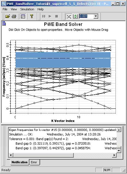
symmetry to speed up calculations. The simulated results are shown in Figure 4.
Figure 4: Band diagram of the rectangular supercell. The defect bands are flat bands within the band gap.
To detect a point defect it is usually enough to run a simulation and ideal lattice, find
band gaps and then run simulation for a defect and a single k-vector. The solutions
within a band gap will be the modes of interest and by a visual check of the field
profiles we can estimate whether the selected supercell domain is large enough.
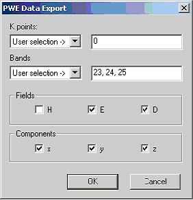
Next step, we what show how can we get the modal field distribution, in the PWE Band Solver Parameters dialog box, k-path section leave only the gamma point and delete all the other major points. Leave the mesh set to 64×64, TE polarization and set the supercell to 5×5 with Domain origin at (3/2,0,3/2). Set number of bands to 30 to account for the first band folding. Click on the File Export button to open the PWE Data Export dialog box (See Figure 5). Select User selection for K points and in the right input field enter the index for the exported k-vector. In this case we run simulation for single k-vector and as the indexing of the k-vector starts from zero enter 0. In Bands section select User Selection. The first band is going to be folded 5×5=25 times, so that index 24 corresponds to the defect. Choose 23, 24, and 25 to export both the defect profiles as well as the profiles of modes below and above the defect. Select all the fields and components for export. Close the dialog box and run simulation.
Figure 5: PWE Data Export dialog box. User specifies k-vectors, bands as well as individual components to be exported.
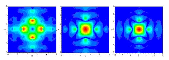
The exported field pattern is in the sub folder where the current project is saved, you
can use our OptiWave 3D viewer to observe these field patterns, and Figure 6 shows
simulated results under different condition.
Figure 6: Localized defect mode of a rectangular lattice of dielectric cylinders (r=0.2, e=8.9) in air. From left to right there are electric field amplitude, magnetic field amplitude of 5×5 supercell and magnetic field amplitude for a supercell 6×6.


