Designing a PBG structure
To design a PBG structure, perform the following procedures.
| Step | Action |
| 1 | Start Waveguide Layout Designer. |
| 2 | To create a new project, select File > New.
The Initial Properties dialog box appears. |
| 3 | Click Profiles and Materials.
The Profile Designer window appears. |
| 4 | Under the Materials folder of OptiFDTD Designer1, right-click the Dielectric folder and select New.
A new Dielectric material dialog box appears. |
| 5 | Type the following information:
Name: PBG_atom Refractive index (Re:): 3.1 |
| 6 | To save the material, click Store.
PBG_atom appears in the Dielectric folder in the directory and in the dialog box title bar. |
To define the channel profile, perform the following procedure.
| Step | Action |
| 1 | Under the Profiles folder of OptiFDTD Designer1, right-click the Channel folder and select New.
The ChannelPro1 dialog box appears. |
| 2 | Create the following channel profile: Profile name: Profile_PBG
2D profile definition Material: PBG_atom 3D profile definition Layer name: layer_01 Width: 1.0 Thickness: 1.0 Offset: 0.0 Material: PBG_atom |
| 3 | Click Store. |
| 4 | Close the Profile Designer. |
To define the wafer and waveguide properties, perform the following procedure.
| Step | Action |
| 1 | In the Initial Properties dialog box, , type/select the following:
Waveguide Properties Width [μm]: 1.0 Profile: Profile_PBG Wafer Dimensions Length [μm]: 21.0 Width [μm]: 15.0 2D Wafer Properties Material: Air 3D Wafer Properties Cladding Thickness [μm]: 1.0 Material: Air Substrate Thickness [μm]: 1.0 Material: Air |
| 2 | Click OK. The Initial Properties dialog box closes. |
Creating the PBG structure
| Step | Action |
| 1 | From the Draw menu, select PBG Crystal Structure. |
| 2 | In the layout window, drag the cursor from a designated starting point and release, to create the PBG area.
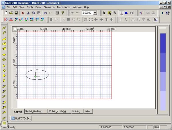
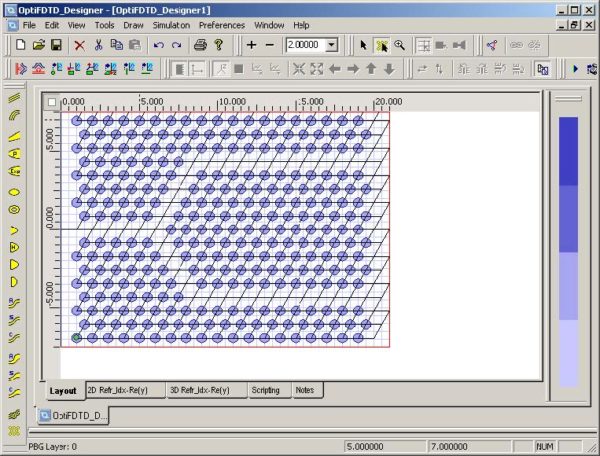
The PBG Crystal Structure appears in the layout window (see Figure 85). |
Figure 85: BPG crystal structure in layout
| 3 | To edit the crystal structure, double-click on the PBG structure in the layout.
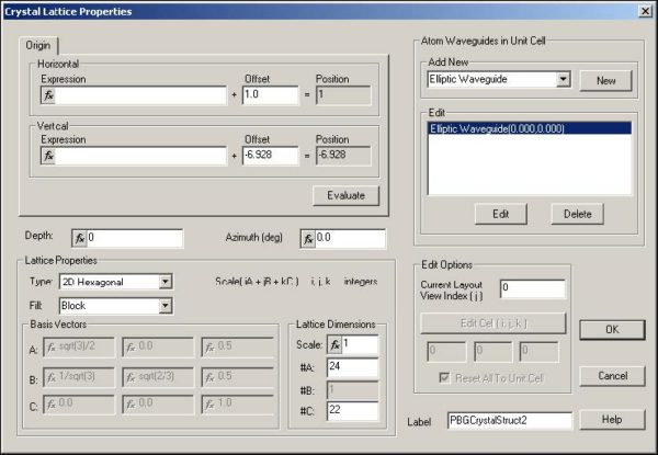
The Crystal Lattice Properties dialog box appears (Figure 86). |
Figure 86: Crystal Lattice Properties dialog box
| 4 | In Origin, Offset, type/select the following:
Horizontal: 1.0 Vertical: -6.928 |
| 5 | Click Evaluate. |
| 6 | Type/select the following:
Depth: 0.0 Azimuth [deg]: 0.0 |
| 7 | In Lattice Properties, Type, select 2D Hexagonal. |
| 8 | In Fill, select Block. |
| 9 | In Lattice Dimensions, type/select the following: Scale: 1.0
#A: 17 #C: 19 Note: When a 2D lattice is selected, the Y-direction cell #B is set to the default value of 1. |
| 10 | In Label, type PBGCrystalStruct1.
Note: Do NOT close the Crystal Lattice Properties dialog box. |
Setting the atom properties
To set the atom properties, perform the following procedure in the Crystal Lattice Properties dialog box.
| Step | Action |
| 1 | In Atom Waveguide in Unit Cell, Add New, select Elliptic Waveguide from the drop-down menu and click New.
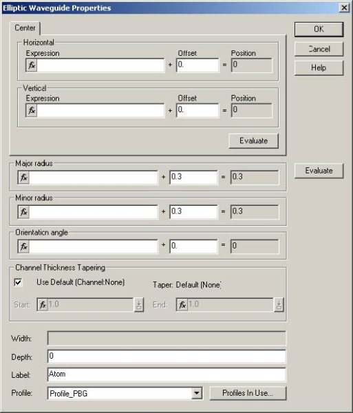
The Elliptic Waveguide Properties dialog box appears (see Figure 87). |
| 2 | In Center, Offset, type/select the following:
Horizontal: 0.0 Vertical: 0.0 |
| 3 | Type/select the following:
Major radius: 0.3 Minor radius: 0.3 Orientation angle: 0.0 Channel thickness tapering: Use Default (Channel: None) Depth: 0.0 Label: Atom Profile: Profile_PBG. |
| 4 | Click OK.
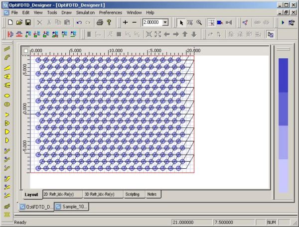
The Elliptic Waveguide Properties dialog box closes. Note: When you return to the Crystal Lattice Properties dialog box, you will see the defined elliptic waveguide listed in Atom Waveguide in Unit Cell. Note: If you close the Crystal Lattice Properties dialog box, you will see the defined PBG structure in the layout window (see Figure 88). |
Figure 87: Elliptic Waveguide Properties dialog box
Figure 88: PBG structure in layout window
There are three ways to create a cell with special properties.
| Step | Action |
| 1 | In the Crystal Lattice Properties dialog box, set the cell position nodes:
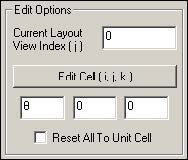
Edit Options i: 8 j: 0 k: 0
|
| 2 | Click Edit Cell (i,j,k) button.
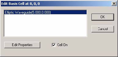
The Edit Basis Cell dialog box appears (see Figure 89). |
Figure 89: Edit Basis Cell dialog box
| Note: To deactivate the basic cell, deselect Cell On. The region will then be recovered to the wafer material. | |
| 3 | Select an atom in the list to edit (in this case, Elliptic Waveguide [5.000,0.000]). |
| 4 | Click Edit Properties.
The Elliptic Waveguide Properties dialog box appears. |
| 5 | Type/select the following:
Major radius: 0.5 Minor radius: 0.4 |
| 6 | Click OK. |
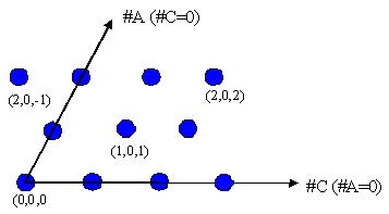
The cell’s index definition for Hexagonal is shown in Figure 90.
Figure 90: Cell index definition for Hexagonal
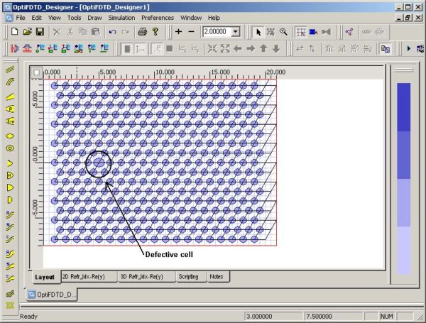
Figure 91: PBG layout with defective cell
OR
| Step | Action |
| 1 | In the layout designer, to select the PBG lattice, click the PBG area.
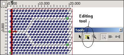
A green dot appears in the PBG structure and the PBG Crystal Structure Cell Editing Tool becomes active. |
| 2 | Select the PBG Crystal Structure Cell Editing Tool icon. |
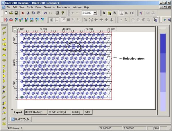
| 3 | Double click on the atom in the Cell (13, 0, 5).
The Elliptic Waveguide Properties dialog box appears. |
| 4 | Type/select the following:
Major radius: 0.4 Minor radius: 0.5 |
| 5 | Click OK to return to the layout window.
The atom at cell (13,0,5) becomes the defective atom (see Figure 92). |
Figure 92: Defective atom at Cell 13,0,5
OR
| Step | Action |
| 1 | In the layout designer, to select the PBG lattice, click the PBG area.
A green dot appears in the PBG structure and the Tools toolbar, including the PBG Crystal Structure Cell Editing Tool, becomes active.
|
| 2 | Select the PBG Crystal Structure Cell Editing Tool, and right-click on the atom in cell (3, 0, 10).
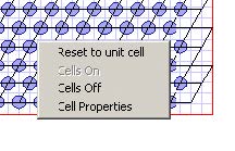
The PBG Cell Edit context menu appears (see Figure 93). |
| 3 | Select Cell Properties. The Edit Basis Cell at 3,0,10 dialog box appears. |
| 4 | Click Edit Properties.The Elliptic Waveguide Properties dialog box appears. |
| 5 | Type/select the following: Major radius: 0.3 Minor radius: 0.3
Figure 93: PBG Cell Edit context menu |
| 6 | In Center, Offset, type/select the following:
Horizontal: 12.2 Vertical: -4.1 |
| 7 | Click OK to close the Elliptic Waveguide Properties dialog box. |
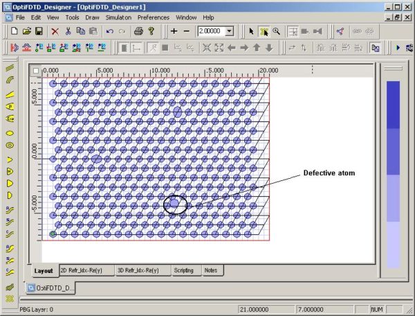
| 8 | Click OK to close the Edit Basis Cell at 3,0,10 dialog box. The atom at cell (3,0,10) becomes the defective atom (see Figure 94). |
Figure 94: Defective atom at Cell 3,0,10
In general, you define the lattice and atom for all the cells in the PBG Lattice Properties dialog box. This is called the Unit cell information. It works like a template; the information in a specified cell is called Basic Cell information. The defect is made in the selected basic cell.
In order to reset defective cells to the unit cell properties, in the Crystal Lattice Properties dialog box, Reset All to Unit Cell must be selected.
Note: If you already tried this, please select Undo in the Edit menu, because the next step in this lesson uses the layout including the defective cells.
Recovering a defective cell at (8, 0, 0) to unit cell
| Step | Action |
| 1 | In the layout designer, to select the PBG lattice, click the PBG area.
A green dot appears in the PBG structure and the Tools toolbar, including the PBG Crystal Structure Cell Editing Tool, becomes active. |
| 2 | Select the PBG Crystal Structure Cell Editing Tool, and right-click on the atom in cell (8, 0, 0).
The PBG Cell Edit context menu appears. |
| 3 | Select Reset to Unit Cell.
The cell values are reset to correspond to the basis cell. |
Now you will create a Y-branch wave path in this PBG layout.
| Step | Action |
| 1 | In the layout designer, to select the PBG lattice, click the PBG area.
A green dot appears in the PBG structure and the Tools toolbar, including the PBG Crystal Structure Cell Editing Tool, becomes active. |
| 2 | Select the PBG Crystal Structure Cell Editing Tool, and right-click on the atom in cell (8, 0, -4).
The PBG Cell Edit context menu appears. |
| 3 | Select Cells Off.
The cell is disabled. |
| 4 | Repeat steps 2 to 3 to disable the following cells:
– (8,0,-3) to (8,0,1) – (9,0,1) to (13,0,1) – (13,0,2) to (13,0,12) – (7,0,2), (6,0,3),(5,0,4), (4,0,5) – (3,0,6) to (3,0,17) |
Figure 95: PBG layout with new wavepath
Now you have finished the PBG layout. The next step is to set up the FDTD simulation.
After you define a lattice, you can use the FDTD band solver to get the preliminary band-diagram ( see “Lesson 9—FDTD Band Solver” on page 269).
The PBG layout can also be defined by using VB scripting. The corresponding sample file for VB scripting can be found in the Samples folder: Sample21_Vbscript_PBG_Layout.FDT.
Inserting the input plane
To insert the input plane, perform the following procedure.
| Step | Action |
| 1 | From the Draw menu, select Vertical Input Plane. |
| 2 | To insert the input plane, click in the layout window where you want it placed.
The input plane appears in the layout. |
| 3 | To edit the input plane, double-click on the input plane in the layout.
The Input Plane Properties dialog box appears. |
| 4 | Set Wavelength to 1.9 μm. |
| 5 | Select Gaussian Modulated Continuous Wave. |
| 6 | On the Gaussian Modulated CW tab, type/select the following: Time Offset [Sec]: 5.5e-14
Half Width [Sec]: 1.1e-14 |
| 7 | On the General tab, select Input Field Transverse: Gaussian. |
| 8 | On the 2D Transverse tab, type/select the following: Center Position [μm]: 0.0
Halfwidth [μm]: 0.8 Tilting Angle [deg]: 0.0 Effective Refractive Index: Local Amplitude [V/m]: 1.0 |
| 9 | On the General tab, type/select the following:
Plane Geometry Z Position [μm]: 1.3 Positive direction |
| 10 | Click OK.
The Input Field Properties dialog box closes. |
Setting up the Observation Point
| Step | Action |
| 1 | From the Draw menu, select Observation Point. |
| 2 | Place the Observation Point in the desired position in the layout. |
| 3 | Double-click the observation point.
The Observation Properties — Point dialog box appears. |
| 4 | On the General tab:
In Center, Offset, type/select the following: Horizontal: 19.5μm Vertical: 4.33μm Center depth: 0.0 μm Label: Observation Point1 |
| 5 | On the Data Components tab, ensure that 2D TE: Ey is selected (default). |
| 6 | Click OK.
The Observation Properties — Point dialog box closes. |
| 7 | Repeat steps 1 to 5 and create another Observation Point with the following information. |
| 8 | On the General tab:
In Center, Offset, type/select the following: Horizontal: 19.5μm Vertical: -4.33μm Center depth: 0.0 μm Label: Observation Point2 |
| 9 | On the Data Components tab, ensure that 2D TE: Ey is selected (default). |
| 10 | Repeat steps 1 to 5 and create another Observation Point with the following information. |
| 11 | On the General tab:
In Center, Offset, type/select the following: Horizontal: 0.8μm Vertical: 0.0μm Center depth: 0.0 μm Label: Observation Point3 |
| 12 | On the Data Components tab, ensure that 2D TE: Ey is selected (default).
Note: Observation Point1 and Observation Point2 are used to get the transmittance, while Observation Point3 is for the reflection. |
Setting the 2D TE FDTD simulation parameters
| Step | Action |
| 1 | From the Simulation menu, select 2D Simulation Parameters.
The Simulation Parameters dialog box appears. |
| 2 | Type/select the following information:
Polarization: TE Mesh Delta X [μm]: 0.1 Mesh Delta Y [μm]: 0.1 |
| 3 | Click Advanced….
The Boundary Conditions dialog box appears. |
| 4 | Type/select the following information:
-X: Anisotropic PML +X: Anisotropic PML -Z: Anisotropic PML +Z: Anisotropic PML Anisotropic PML Calculation Parameters Number of Anisotropic PML Layers: 10 Theoretical Reflection Coefficient: 1.0e-12 Real Anisotropic PML Tensor Parameters: 5.0 Power of Grading Polynomial: 3.5 |
| 5 | In Time Parameters, click Calculate.
The default time step size is calculated. |
| 6 | Select Run for 10000 Time Steps (Results Finalized). |
| 7 | Select Key Input Information: Input Plane1 and wavelength:1.9.
Note: The input plane’s center wavelength is used for DFT calculations. |
| 8 | Click OK to close the Simulation Parameters dialog box without running the simulation, or click Run to start the OptiFDTD Simulator.
Note: Before running the simulation, save the project to a file. |
Observing the simulation results in OptiFDTD Simulator
Key things to observe:
- Refractive index distribution
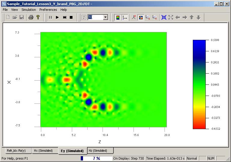
- Observe the wave propagation in OptiFDTD Simulator (see Figure 96)
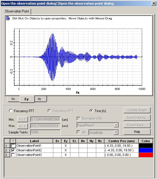
- Select View > Observation Point to observe the dynamic time domain and frequency domain response (see Figure 97).
Figure 96: Wave propagation in OptiFDTD Simulator
Figure 97: Dynamic time domain and frequency domain response
Performing data analysis
In OptiFDTD_Analyzer, you can perform the following analysis for this sample:
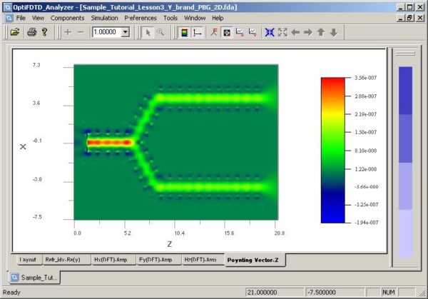
- Observe the Layout, Refractive index, Poynting Vector, and field propagation pattern (DFT results) for the center wavelength (see Figure 98 for Poynting Vector-Z).
Figure 98: OptiFDTD Analyzer
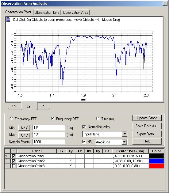
- Observe the transmission/reflection calculations
| Step | Action |
| 1 | To start the observation point analysis, from the Tools menu, select
Observation Area Analysis. The Observation Area Analysis dialog box appears (see Figure 99). |
| 2 | Select ObservationPoint1 and ObservationPoint2.
The simulation results from the observation points displays in the graph window. |
| 3 | Type/select the following:
Frequency DFT Min. λ /f : 1.5μm Max. λ /f : 2.3μm Sample Point: 1000 Normalize With InputPlane1 dB Amplitude |
Figure 99: Observation Area Analysis dialog box


