Create a new project
The following lesson uses a micro-ring resonator as a sample design.
Note: The corresponding project file can also be found in the Sample’s file folder, Sample02_3D_Ring_Resonator.fdt.
To create a new project, perform the following procedures.
Opening OptiFDTD_Designer
| Action | |
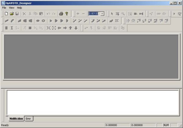
| To open OptiFDTD_Designer, from the Start menu, select Programs > Optiwave Software > OptiFDTD > Waveguide Layout Designer.
OptiFDTD_Designer appears. |
Figure 1: OptiFDTD_Designer
Initializing the project
| Action | |
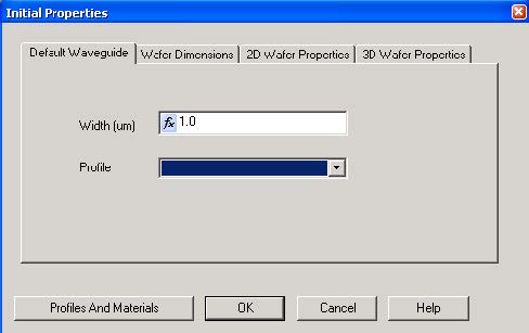
| To initialize the project, from the OptiFDTD_Designer File menu, select New.
The Initial Properties dialog box appears |
Figure 2: Initial Properties dialog box
Opening the Waveguide Profile Designer
| Step | Action |
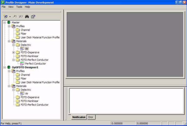
| 1 | To define the materials, in the Initial Properties dialog box, click Profiles And Materials.
The Waveguide Profile Designer opens. |
Figure 3: Waveguide Profile Designer
Note: You can also open the Waveguide Profile Designer from the Start menu (see “Opening OptiFDTD_Designer” on page 99).
Defining the material
| Step | Action |
| 1 | In the directory under OptiFDTD_Designer1, Materials folder, right-click the Dielectric folder.
A context menu appears. Figure 4: Context menu |
| 2 | Select New.
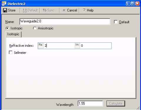
The Dielectric dialog box appears. Figure 5: Dielectric dialog box |
| 3 | Type the following information
Name: Waveguide2.0 Refractive index (isotropic)(Re): 2.0 |
| 4 | To save the material, click Store. To close the dialog box click |
Defining the 2D and 3D channel profile
| Step | Action |
| 1 | In the directory under OptiFDTD_Designer1, under the Profiles folder, right-click the Channel folder.
A context menu appears. |
| 2 | Select New.
The Channel Profile dialog box appears. |
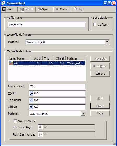
Figure 6: ChannelPro1 dialog box
| 3 | Type the following Profile name: waveguide |
| 4 | To define the 2D profile, in the Material list under 2D profile definition, select Waveguide2.0. |
| 5 | To define the 3D profile, under 3D profile definition:
a. Type the following information: Layer name: WG Width: 0.5 Thickness: 0.5 Offset: 0. b. In the Material list, select Waveguide2.0 c. Click Add. |
| 6 | To save the channel profile, click Store.
Waveguide appears in the Channel folder in the directory, in the dialog box title bar, and on the tab at the bottom of the layout. |
| 7 | To return to OptiFDTD_Designer, either minimize or close the Waveguide Profile Designer. |
Setting up the initial properties
To set up the initial properties, perform the following procedure.
| Step | Action |
| 1 | In the Initial Properties window, click the Waveguide Properties tab. |
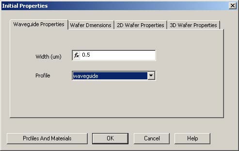
| 2 | Type the following value: Width (μm): 0.5 |
| 3 | From the profile list, select waveguide. |
Figure 7: Initial Properties dialog box—Waveguide Properties tab
| 4 | Click the Wafer Dimensions tab. |
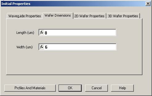
| 5 | Type the following value:
Length (μm): 8 |
Figure 8: Initial Properties dialog box—Wafer Dimensions tab
| 6 | Click the 2D Wafer Properties tab. |
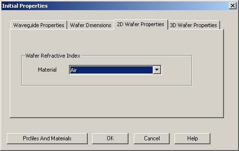
| 7 | From the Material list, select Air. |
Figure 9: Initial Properties dialog box—2D Wafer Properties tab
| 8 | Click the 3D Wafer Properties tab. |
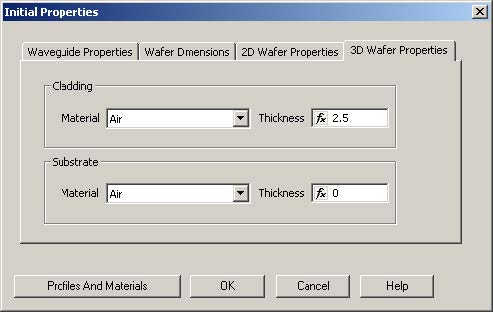
Figure 10: Initial Properties dialog box—3D Wafer Properties tab
| 9 | Under Cladding, from the Material list, select Air. |
| 10 | Under Substrate, from the Material list, select Air. |
| 11 | Type the following values:
Cladding thickness (µm): 2.5 Substrate thickness (µm): 0 Note: Cladding and substrate are two layers in the Y-direction that can have different materials and thicknesses. The Y-axis origin is at the interface between the substrate and cladding. |
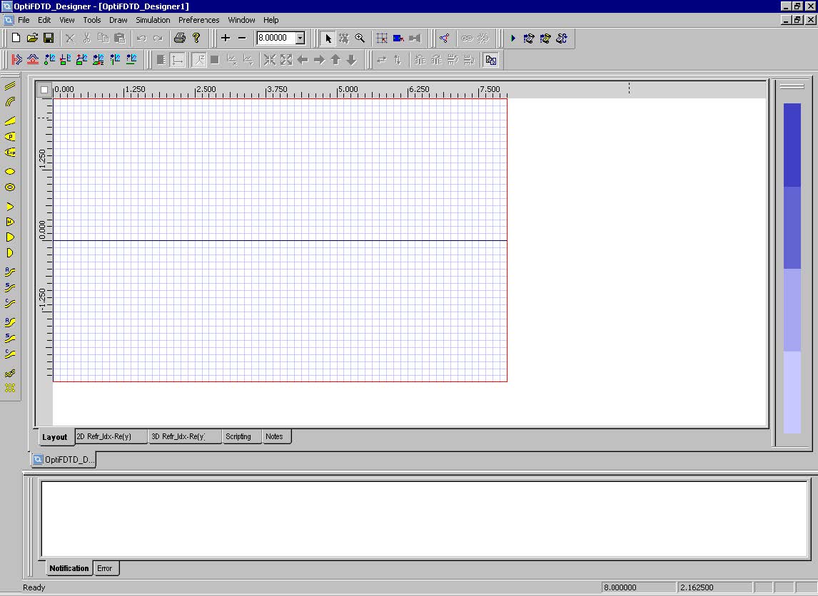
| 12 | To finish the initial properties setup, click OK.
The layout window appears. Note: Click Zoom tool to enlarge the layout window. |
Figure 11: Layout window


