To insert the Input Plane and set the excitation, perform the following procedures.
Inserting the Input Plane
| Step | Action |
| 1 | From the Draw menu, select Vertical Input Plane.
Note: – The Vertical Input Plane is in the x-y plane for 3D. – The Horizontal Input Plane is only functional with a 2D simulation. – Multiple Input Planes are only allowed in a 2D simulation. |
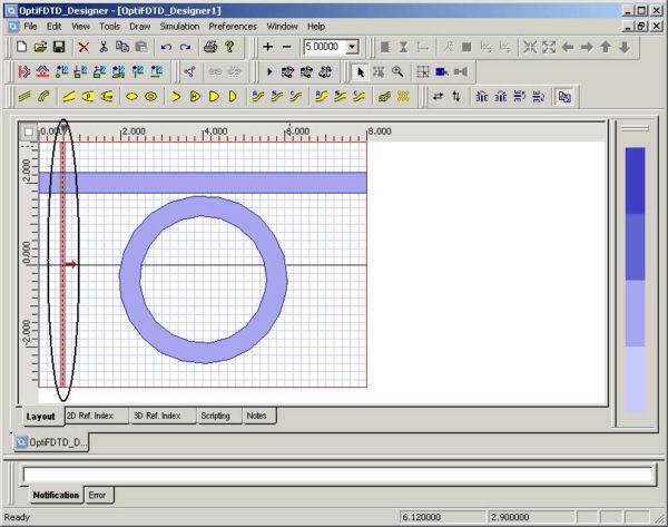
| 2 | Click in the layout window at the position where you want to insert the Input Plane. A red line that presents the input plane appears in the layout window. |
Figure 19: Input Plane
| 3 | To set up the Input Plane properties, double-click the red line (Input Plane) in the layout window.
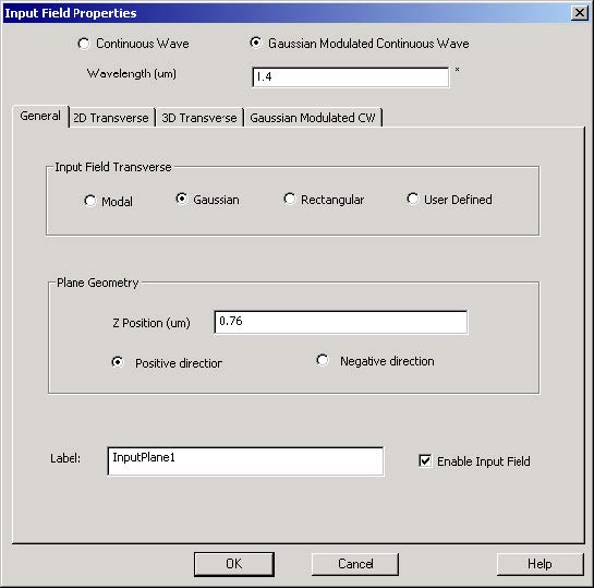
The Input Field Properties dialog box appears. |
Figure 20: Input Field Properties dialog box
| 4 | Set the time domain Input Plane information.
a. Select Gaussian Modulated Continuous Wave. The Gaussian Modulated CW tab appears. b. Wavelength (µm): 1.4 Note: – For Continuous Wave, Wavelength is the single wavelength to be simulated. – For Gaussian Modulated Continuous Wave, Wavelength is the carrier wavelength (center wavelength) for the pulse. |
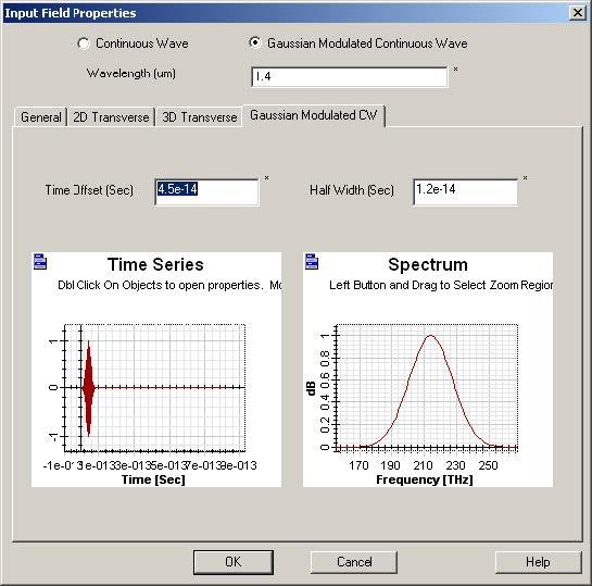
| 5 | Click the Gaussian Modulated CW tab.
The time domain pulse graphics appear. |
| 6 |
Type the following values for the time domain input plane. Time offset (sec.): 4.5e-14 Half width (sec.): 1.2e-14 |
Figure 21: Gaussian Modulated CW tab
| Note:
– Both the time domain wave and frequency domain wave for the Input Plane appear. – The Frequency domain information is obtained by FFT from the time domain series. – Right clicking on the graph allows you to select the graph tools. – Time offset controls the time domain beam center. – Half width controls the beam size and bandwidth. |
|
| 7 | To set up the general information (transverse field distribution) for the Input Plane, click the General tab.
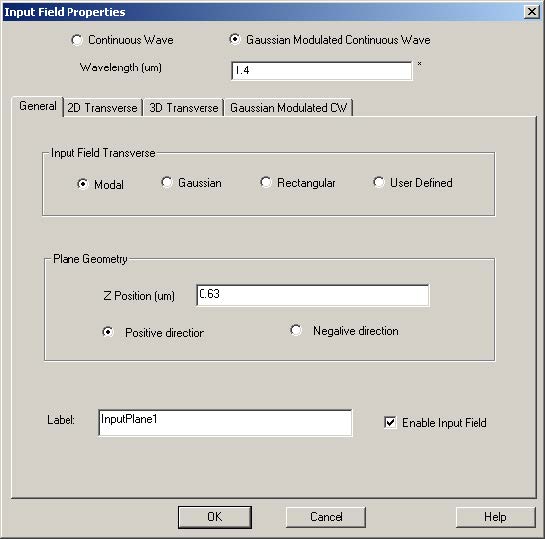
a. Input Field Transverse: Modal b. Z Position (µm): 0.63 c. Plane Geometry: Positive direction d. Label: InputPlane1 (default) |
Figure 22: General tab
Note: Positive Direction means the that the Input Plane is excited to the
positive z-direction. Negative Direction means that the Input Plane is excited
to the negative z-direction.
| 8 | To solve the 3D transverse mode, click the 3D Transverse tab. |
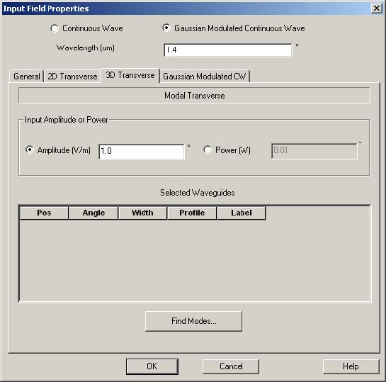
Figure 23: 3D Transverse tab
| 9 | Type the following Input Amplitude value (V/m): 1.0 |
| 10 | Click Find Modes.
The Waveguide selection window appears. |
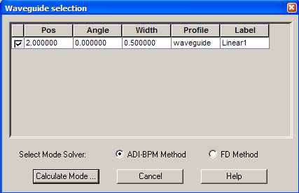
Figure 24: Waveguide selection dialog box
| 11 | Select the Linear Waveguide check box, select ADI-BPM Method. |
| 12 | To open the mode solver, click Calculate Mode.
The Globe Data: ADI Method dialog box appears. |
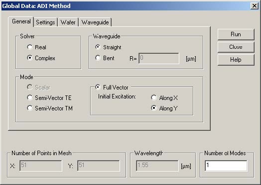
Figure 25: Global Data: ADI Method dialog box
| 13 | Set the following:
Solver: Complex Waveguide: Straight Mode (initial excitation): Full Vector, Along Y Wavelength (µm): 1.4 (the same as the input wavelength by default, Read-Only) Number of Modes: 1 |
| 14 | Click the Settings tab and set Boundary Condition: TBC |
| 15 | To solve the mode, click Calc. Mode.
The 3D Mode Solver opens. |
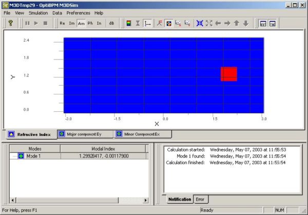
Figure 26: 3D Mode Solver
| Note:
– The 3D Mode Solver can take a while to start up. – It can take several minutes to solve the mode. – A message appears to advise you if no mode has been found. |
|
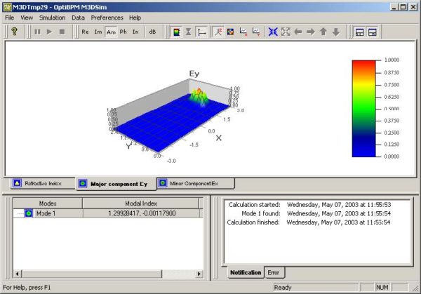
| 16 | After solving the mode, click the field (Ex, Ey) tab to view the field pattern. |
Figure 27: Major component Ey tab
| 17 | To return to the Input Field Properties dialog box, close the 3D Mode Solver. |
| 18 | To complete the Input Plane setup, click OK. |
Saving the layout
To save the layout you have created, perform the following procedure.
Note: Do not save your project over the sample file provided.
| Step | Action |
| 1 | From the File menu, select Save As.
The SaveAs dialog box appears. |
| 2 | In the sample folder, enter the name of the file and click Save.
The new sample file is saved in the sample folder.
Note: .fdt is the file extension generated by OptiFDTD_Designer. |


