Metallic and lossy materials in solar cells or other semiconductor devices in general absorb part of the light wave energy, converting it to heat. This lesson demonstrates the heating absorption simulation in OptiFDTD.
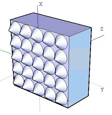
The layout we will simulate is shown in Figure 1, the corresponding project file (Sample44_3D_Heating_Absorption_64bit.fdt) can be found under the Sample folder of your software installation directory
Sample44_3D_Heating_Absorption_64Bit.fdt.
The layout represents a square of periodic cones with height (z-direction length) of
1μm deposited on the flat substrate. The diameter of the cone’s bottom is 1μm, the
394
cone and substrate have the same refractive index which is n=2.4-j0.056. The cone
lattice extends to infinity in x and y-direction, the input wave is the plane wave with
zero tilting angle. In this case a 5X5 cone layout is taken for simulation with the x- and
y-edge set as periodic boundary condition. The following are the detailed steps for
the layout creation, simulation, and post-simulation analysis.
Layout creation steps
| Step | Action |
| 1 | Open OptiFDTD Waveguide layout Designer
From the Start menu, select Programs –>Optiwave Software –> OptiFDTD –> Waveguide Layout Designer. OptiFDTD_Designer window opens. |
| 2 | Create a new project.
From the OptiFDTD_Designer File menu, select New. The Initial Properties dialog box appears. |
| 3 | Define the material(s) and waveguide profile(s) that will be used in the project.
Click the Profiles and Materials button in the Initial Properties dialog. The Profile Designer OptiFDTD opens. Note: At any time, you can open the Profile Designer from the “Edit->Profiles and Materials…” menu of the Layout Designer or from the Start menu. So you can make appropriate modifications to the defined materials and profiles whenever it is needed. a. In the three listing of profiles and materials of Profile Designer under OptiFDTD_Designer1 in the Materials folder, right-click the Dielectric folder. A context menu appears. Select New, the Dielectric dialog box appears. By default the constant refractive index (Const Ref. Idx) is selected. Type the following information: • Name: n=2.4-j0.056 • Constant refractive index (isotropic): (Re): 2.4, (Im): 0.056 • Click Store to save this material, Material n=2.4-j0.056 will be listed under the • Dielectric folder b. In the directory under OptiFDTD_Designer1, under the Profiles folder, right click the Channel folder. A context menu appears. Select New. The Channel Profile dialog box appears. Type the following information: • Profile name: ChannelPro1 • Under 3D profile definition: Type the following information: Layer name: Layer1 Width: 5 Thickness: 5 Offset: 0.0 • In the Material list, select n=2.4-j0.056 • Click Add. • To save the channel profile, click Store. ChannelPro1 appears in the Channel folder, c. In the directory under OptiFDTD_Designer1, under the Profiles folder, right click the Fiber folder. A context menu appears. Select New. The Fiber Profile dialog box appears. Type the following: •Profile name: FiberPro1 •Under 3D profile definition: Type the following information: Layer name: Layer1 Rx (x-direction radius): 0.5 Ry (y-direction radius): 0.5 •In the Material list, select n=2.4-j0.056 •Click Add. • To save the channel profile, click Store. FiberPro1 appears in the Channel folder, |
| 4 | Return to Initial Properties dialog box of Waveguide Layout Designer Either minimize or close the Waveguide Profile Designer. |
| 5 | Type the following information in each corresponding area in Initial Properties dialog box
• Waveguide Properties: Width (um): 1.0 Profile: FiberPro1 (This profile will be used by default when drawing a waveguide in the layout window) • Wafer Dimension Length (um): 5.0 (z-direction dimension) Width (um): 5.0 (x-direction dimension) • 3D Wafer Properties Cladding Material: Air Cladding Thickness: 5 (y-direction dimension) Substrate Material: Air Substrate Thickness: 0 (y-direction dimension) |
| 6 | Click OK in Initial Properties dialog box. OptiFDTD Designer- [OptiFDTDigner1] window appears.
Note: • If not all Toolbars appear in the Layout Desinger window, you can change it from the “View->Toolbars” menu option. • Click “+” (zoom) toolbar button to enlarge the layout window. • Open “Wafer Properties” from the Edit menu to modify simulation domain properties. • Select “Profiles and Materials” from the Edit menu to open the Profile Designer where you can add and modify materials and profiles. |
| 7 | Draw a linear waveguide (the substrate in Figure 1) in the layout window
• From the Draw menu, select Linear Waveguide. Or select the Linear Waveguide shortcut toolbar. • In the layout window, drag the linear waveguide from the start point to the end point. A linear waveguide appears in the layout window.(Change the mouse drawing tool by selecting the arrow shortcut icon on the toolbar) • To adjust the position and the shape of the waveguide, in the layout window, double-click the Linear Waveguide. The Linear Waveguide Properties dialog box appears. • From the Profile list, select ChannelPro1. • Click the Start tab and type the following values: Horizontal offset (um): 3.0 (Start point for z-direction) Vertical offset (um): 0.0 (Start point for x-direction) • Click the End tab and type the following values: Horizontal offset (um): 5.0 Vertical offset (um): 0.0 • Channel Thickness Tapering: Use Default (Channel: None): Uncheck Taper: Linear Start: 5 End: 5 • Width (um): 5.0 (Waveguide x-direction width) • Depth (um): 0.0 (Waveguide y direction bottom) • Label: Linear1 • Click OK to finished the waveguide setting Note: • You can parameterize the waveguide by entering a user-defined variable (parameter) in the Expression field. The expression fields are marked with “fx”. For example you can enter StartPosZ (or an expression like 2*StartPosZ), in the Expression field of Horizontal position definition. After that press the Evaluate button, to see the resulting Position value. If the specified parameter has not been defined, then the software will prompt you to define it. • Horizontal means the z-direction. • Vertical means the x-direction. • Depth means the y-direction. |
| 8 | Draw Cones
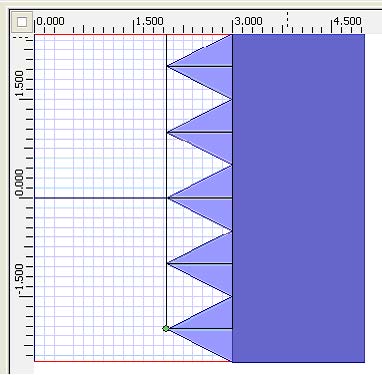
• From the Draw menu, select PBG Crystal Structure. • With the mouse cursor click once on the layout window, The PBG Crystal Structure appears in the layout window. Click Select tool button (the arrow) on the shortcut toolbar to release the PBG selection. • Double-click on the PBG structure (a rectangular shape) on the layout. The Crystal Lattice Properties dialog box appears. • In the Crystal Lattice Properties dialog box, set the following lattice reference position parameters: Origin Horizontal Offset: 2.0 Vertical Offset: -2.0 Depth: 0.5 • In the Crystal Lattice Properties dialog box, set the following Lattice vector parameters: Lattice Properties: Type: 3D rectangular Fill: Block Lattice Dimension: Scale: 1.0 #A: 5 #B: 5 #C: 1 • In the Crystal Lattice Properties dialog box, set the Atom Waveguide ( Cone) properties: In Atom Waveguide in Unit Cell, Add New, select Linear Taper Waveguide from the drop-down menu and click New. The Linear Taper Waveguide Properties dialog box appears. In Linear Taper Waveguide Properties dialog box set following value: Profile: FiberPro1 Start Horizontal Offset: 0 Vertical Offset: 0 End Horizontal Offset: 1 Vertical Offset: 0 Fiber Diameter Tapering User Default (checked) Width Click OK to close the Linear Taper Waveguide setting. • In the Crystal Lattice Properties dialog box, click OK to close the Crystal Lattice setting. The layout creation is finished; the layout window should like the Figure 2 |
Figure 2: Layout in OptiFDTD


