Grating layouts in most cases are the periodic structure. There are two ways in OptiFDTD to realized the periodic layout: PBG editor and VB scripting, PBG layout and corresponding simulations are discussed in Lesson 3, Lesson 11 – 14. This lesson will focus the following features:
• Using VB scripting to generate the grating (or periodic) layout.
• Grating layout simulation and post-processing analysis
Note: It is assumed that you are familiar with Lesson 1—Getting started and with material and profile definition.
Introduce the layout
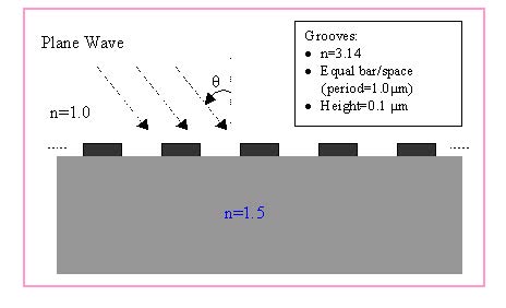
We are going to simulate a 2D grating layout that is shown in the Figure 1.
Figure 1: Layout
Note: Note: The corresponding project file can also be found in the Sample file folder, Sample37_2D_VB_Script_Grating.FDT
Define a 2D grating layout with VB scripting
| Step | Action |
| 1 | Start a new project from Waveguide Layout Designer by select “New” in the file menu.
Initial Properties dialog box appears |
| 2 | In the Initial Properties dialog box set the following parameters:
Wafer Dimensions Length (mm): 8.5 Width (mm): 3.0 2D wafer properties: Wafer refractive index: Air |
| 3 | Click Profiles and Materials.
The Profile Designer window appears. |
| 4 | Click Profiles and Materials.
In the Profile designer, under the folder “OptiFDTD_Designer1”, define and store the following dielectric materials. Name: N=1.5 Refractive index (Re:): 1.5 Name: n=3.14 Refractive index (Re:): 3.14 |
| 5 | In the profile designer, under the folder OptiFDTD_Designer1, define the following channel profiles:
Name: ChannelPro_n=3.14 2D profile definition, Material: n=3.14 Name: ChannelPro_n=1.5 2D profile definition, Material: n=1.5 |
| 6 | In the Initial Properties dialog box, Set ChannelPro_n=3.14 as the default profile, and click “OK” to start the main designer OptiFDTD_Designer windows appears |
| 7 | In the OPtiFDTD_Designer window, Draw the following Objects
a. Linear waveguide 1 Label: linear1 Start Horizontal offset: 0.0 Start vertical offset: -0.75 End Horizontal offset: 8.5 End vertical offset: -0.75 Channel Thickness Tapering: Use Default Width: 1.5 Depth: 0.0 Profile: ChannelPro_n=1.5 b. Linear waveguide 2 Label: linear2 Start Horizontal offset: 0.5 Start vertical offset: 0.05 End Horizontal offset: 1.0 End vertical offset: 0.05 Channel Thickness Tapering: Use Default Width: 0.1 Depth: 0.0 Profile: ChannelPro_n=3.14 |
| 8 | In the In the OPtiFDTD_Designer window, define an horizontal input plane with following properties:
Continuous Wave Wavelength: 0.63 General: Input field Transverse: Rectangular X Position: 0.5 Direction: Negative Direction Label: InputPlane1 2D Transverse: Center Position: 4.5 Half width: 5.0 Titlitng Angle: 45 Effective Refractive Index: Local Amplitude: 1.0 |
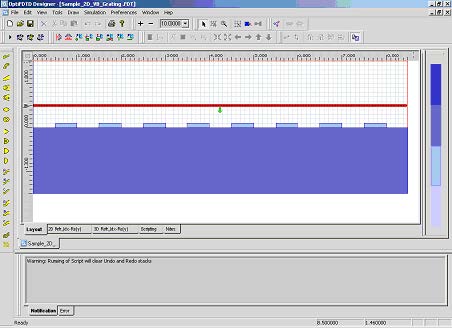
Figure 2: OptiFDTD Designer window after Step 8.
| 9 | Click “Layout Script” Shortcut tool bar or select “Generate Layout Script…” under the Simulation menu. This step will transform the layout object to the VB scripting code. The software will ask: “Generate Layout Script? This will overwrite the current script.” Click Yes.
The Scripting page appears |
| 10 | Click “Layout” button to go to the Layout window, and delete all the objects in the layout window. |
| 11 | Click “ Test Script” shortcut toolbar or select “Test Script” in the Simulation Menu. This will run the VB script code.
Now all the designed objects come back from VB scripting code. The layout should look like figure 2 (This steps shows that the layout can be designed by VB script) |
| 12 | Click “ Scripting” button to go to the scripting page. Modify the Linear2 code paragraph as the following:
Dim Linear2 for m=1 to 8 Set Linear2 = WGMgr.CreateObj ( “WGLinear”, “Linear2″+Cstr(m) ) Linear2.SetPosition 0.5+(m-1)*1.0, 0.05, 1+(m-1)*1.0, 0.05 Linear2.SetAttr “WidthExpr”, “0.1” Linear2.SetAttr “Depth”, “0” Linear2.SetAttr “StartThickness”, “0.000000” Linear2.SetAttr “EndThickness”, “0.000000” Linear2.SetProfileName “ChannelPro_n=3.14” Linear2.SetDefaultThicknessTaperMode True |
| 13 | Click “ Test Script” shortcut toolbar to run the Modified VB script code. The grating layout is generated, the layout is shown in Figure 3. |
Figure 3: Grating layout generated by VB scripting after Step 13.
Note: As has been demonstrated:
a. VB scripting provides a way to generate the periodic layout.
b. VB script can also design other objects that can be draw in the layout. such as input plane, Observation Objects.
c. For more detail information about VB scripting, please refer to the VB Scripting Reference.
Make sure you save the layout.
Setup simulation parameters
| Step | Action |
| 1 | Select “ 2D simulation parameters…” under the Simulation menu Simulation Parameters dialog box appears |
| 2 | In the Simulation Parameters dialog, set up the following parameters:
TE simulation Mesh Delta X: 0.015 Mesh Delta Z: 0.015 Time Step Size: Auto Run for 1000 Time steps |
| 3 | Click Advanced Button to set up the Boundary condition Set X and Z edge as Anisotropic PML boundary condition.
Number of Anisotropic PML layers: 15 Set other parameters with default value. |
Perform the simulation
• Click Run button in the Simulation Parameters to start the Simulation
• In the Analyzer, the time domain response for each field components can be observed.
• After the simulation, click “Yes” to start the Analyzer.
Perform far field analysis for the diffraction wave.
| Step | Action |
| 1 | In the OptiFDTD Analyzer, select “Crosscut Viewer” in the Tools Crosscut Viewer window appear |
| 2 | In the crosscut viewer, select “ Definition of the Cross Cut” as z-direction. |
| 3 | Move the slice position to mesh point equal to 92, ( Position: -0.12) Observe the near field in the current slice |
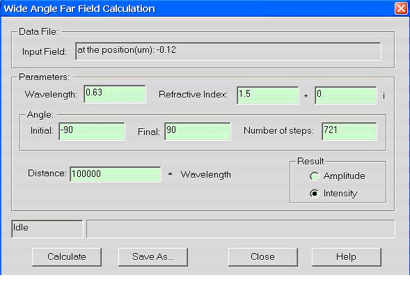
| 4 | Select “Far Field” in the tools menu of cross cut viewer. Far field transform dialog box appears. (Figure 4) |
Figure 4: Far-field Calculation dialog box
| 5 | In the Far Field Calculation dialog box. Set up the following parameters.
Wavelength: 0.63 Refractive index: 1.5+0i Angle Initial: -90.0 Angle Final: 90.0 Number of Steps: 721 Distance: 100, 000*wavelength Intensity |
| 6 | Click “Calculate” button to start the calculation and save the results as
Farfield.ffp. |
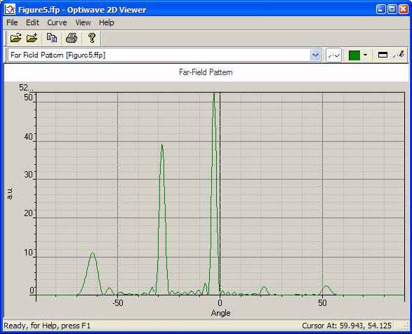
| 7 | Start the “Opti 2D Viewer” and load the Farfield.ffp. The far field is shown in Figure 5. |
Figure 5: Far field Pattern in “Opti 2D Viewer”


