1.1 Create a 3D rectangular lattice of dielectric spheres
Note:
– In this lesson, it is assumed that you already read the PWE tutorial Lesson 11 – Analyzing 1D Photonic Crystals (Bragg gratings) and Lesson 12 – Analyzing 2D Photonic Crystals.
– For the details on how a lattice can be created, please refer to Lesson 3— Photonic crystal and photonic band gap simulation and Lesson 9—FDTD Band Solver.
– For the details on how material and waveguide profile can be created, please refer to tutorial Lessons 1 through to Lesson 9.
– To define the variable, please input the variable name in the Initial Properties dialog box. Click OK to access the Variables and Function dialog box to define the values.
When a project is initialized, in the profile designer, please define two constant materials with name as “Air” and “eps13”, and the refractive index as 1.0 and 3.6055 respectively. . As the air is already predefined as a default material we only need to create one new material with refractive index of ~3.6055.
Please also define a channel default profile use Air or eps13. OptiFDTD layout designer requires this default even though you will not need it to build the photonic crystal.
In the project initial properties dialog box, Please define wafer dimensions as 5×5 microns, cladding material as eps13 and thickness 3 micron, substrate material eps13 and thickness 1micron.
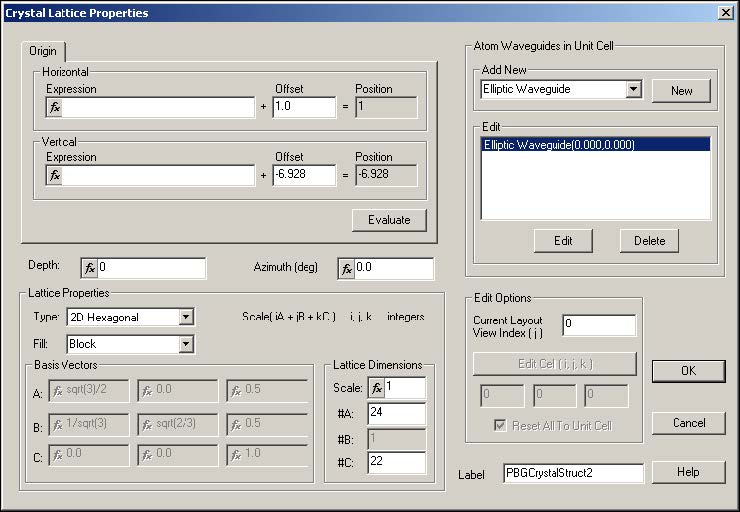
In the layout designer click on the PBG Crystal Structure icon and place a lattice structure on a layout. Open Crystal Lattice Properties dialog box and specify Lattice Type as FFC. The lattice vectors will be automatically generated. Make sure the scale is set to 1.0 and number of lattice vector translations is set as (#A,#B,#C)=(3,3,3).
(See Figure 1)
Figure 1: Crystal lattice Properties dialog box.
Enter new 3Dsphere object in the Atom Waveguides in Unit Cell. Edit the properties
of the Sphere objects by setting the radius of 0.3716 and its material to Air. Return to
the layout designer. Check the refractive index in the refractive index viewer and
persuade yourself you created FCC lattice of air spheres submerge in dielectric.
1.2 Set simulation parameters
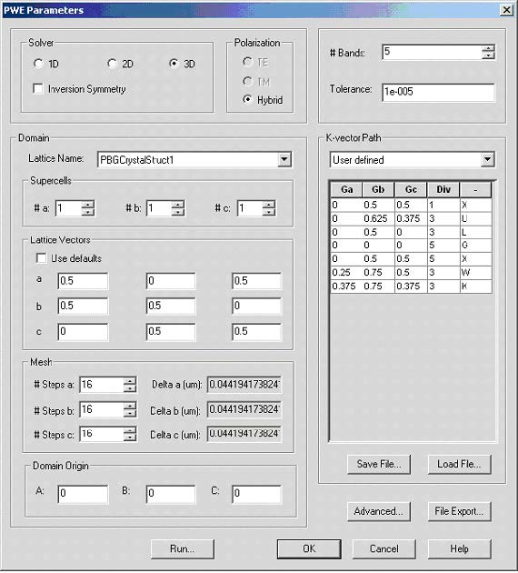
Open the PWE Simulation Parameters dialog box and set 3D solver. Hybrid
polarization option will be automatically selected. The current version does not allow
applying any symmetry constraints in 3D simulations. As our lattice vectors in case of
FCC lattice are not standard FCC lattice vector, we want to set the lattice vectors for
PWE simulation manually so that they correspond to the standard way. Uncheck the
Use Defaults and set vectors as:
a=(0.5, 0.0, 0.5)
b=(0.5, 0.5, 0.0)
c=(0.0, 0.5, 0.5)
In this simulation use the mesh resolution as 16x16x16. To increase accuracy you might want to increase the mesh size later. The simulation time will significantly increase.
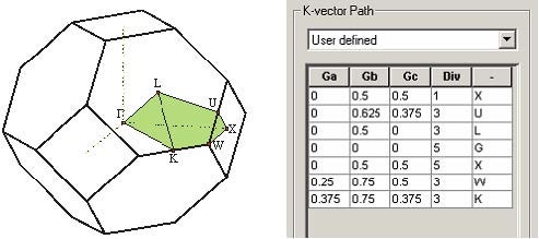
Next step is to define the k-path in terms of the reciprocal vectors. In this case we want to scan the irreducible first Brillouin zone. The definition of the points of higher symmetry will define the zone can be found elsewhere. The symmetry point, we will define are shown in Figure 2.
Figure 2: Schematic of the first Brillouin zone of FCC lattice (truncated octahedron) with high symmetry points (left) and defined k-path across the irreducible Brillouin zone (right).
To edit the k- path, Please choose the “User defined” in the K-Vector Path list, then right click on the k-path area, and select “Add” to edit the terminal point or stop point for a k-vector path.
Figure 3 shows the PWE simulation parameter dialog box.
Figure 3: PWE simulation parameters dialog box
Add an input wave plane in the layout, and then you can perform the PWE band solver
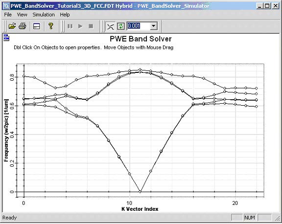
simulation. The resulting band structure does not contain any complete band gap.
Similar results can be found for example in reference [1][2]. (See Figure 4).
Figure 4: Hybrid band structure of FCC lattice (mesh16*16*16)


