Note:
- For the details on how a lattice can be created, please refer to Lesson 3— Photonic crystal and photonic band gap simulation and Lesson 9—FDTD Band Solver.
- For the details on how material and waveguide profile can be created, please refer to Lessons 1 through to Lesson 9.
We start investigating system of equally thick alternating layers with dielectric constants e1=13 and later on we will change layer thickness ratio. Open a new project. Create new materials named ‘eps13’ with constant isotropic refractive index of 3.6056. Material “Air” is a default material in OptiFDTD and will be used in this project. Here we use the relationship between refractive index and permittivity ε = n2 . We will also need a channel profile with permittivity eps13. Create a new channel profile named ‘chan_eps13’ and specify its 2D refractive index as eps13. In this tutorial we will not use 3D profile definition.
It is a good practice to parameterize the layout design so that later modifications can
be done in a fast and flexible way. We will first create several variables, which will
represent some of the physical properties of the design.
| lngth | 10 | Layout lenght |
| wdth | 10 | Layout width |
| offset | 0.0 | Horizontal offset of the unit cell elements from the lattice point (important in case of exploiting inversion symmetry). |
| scale | 1.0 | Scale factor – scales grating dimensions. |
| a | 0.5 | ac will define width of a Bragg layer (c is lattice vector). |
Table 1
Note: To define the variable, please input the variable name in the Initial Properties dialog box. Click OK to access the Variables and Function dialog box to define the values.
Finish the initial steps by defining wafer, cladding and default waveguides as follows:
– Default profile: chan_eps13
– Waveguide width: wdth
– Wafer dimensions: lngth / wdth
– 2D Wafer: Air
Save the project under a new name.
There are several ways how to create a Bragg grating structure. You can create the structure by placing individual waveguides on the layout one by one, using script or lattice generator. We use the lattice generator to create 1D lattice with alternating layers represented by simple linear waveguides surrounded by air.
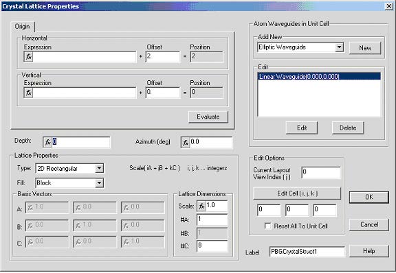
In the layout designer create a new PBG Crystal structure, double click on it to open the Crystal Lattice Properties dialog box. Use the default 2D rectangular lattice and specify the Lattice dimensions #A=1 and #C=8. This will create 1D lattice with 8 unit cells along C vector direction. Center the lattice on the layout by setting the origin as (2, 0) (horizontal, vertical). See Figure 1.
Figure 1: Crystal lattice Properties dialog box
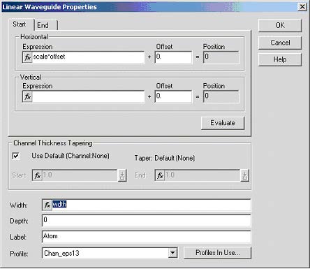
Add new linear waveguide atom to the unit cell. Now you need to edit the properties
of the linear waveguide. As the atom uses absolute coordinates we have to use our
scale variable to preserve scalability of the design. Set the linear waveguide position.
(See Figure 2)
Figure 2: Atom—Linear Waveguide Properties Dialog box
– Start horizontal: scale*offset
– Start vertical: 0.0
– End horizontal: scale*(offset+a)
– End vertical: 0.0
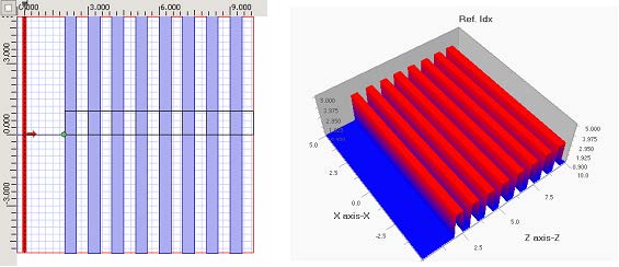
Select chan_eps13 profile. Get back to the layout designer. Put vertical input plane in the z-position of 1.0um. Check the layout and refractive index visually. Persuade yourself that the design will scale when you change the scale factor scale. You can also experiment with the filling factor a. To view the refractive index you need to enter an input plane to the design.
Figure 3: Layout design (left) and refractive index view (right)
When you are finished experimenting make sure that a=0.5 and scale=1.0. To get
final band diagrams in the same form as in the [1] we chose the lattice constant to be
1.


