Thanks to the parameterized design we can easily verify other published results as
well as point out other features of PWE band solver. Let’s change a variable to 0.2 to
simulate grating with alternating layers of different widths. The layer of the high
permittivity (waveguides) will be 0.2a thick, whereas the air layer will be 0.8a thick (for
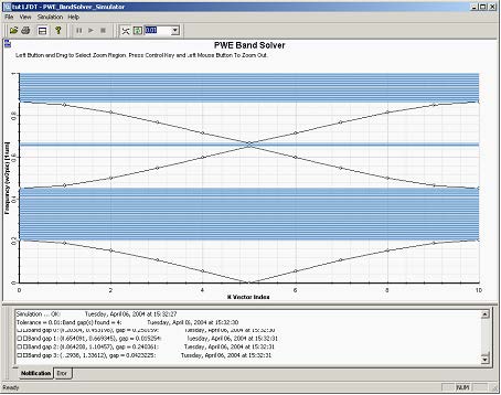
scale=1). Below you see the resulting band structure as reported in reference [1].
Figure 6: Band structure of the Bragg grating with dielectric layers of thickness 0.2 mm (period =1mm, permittivity 13.0/1.0).
The calculated eigenfrequencies are plotted in a normalized fashion as,
![]()
in units [1/mm], which is not the same as usually reported results in a non-dimensional form ![]() . To get the non-dimensional results, you need to scale the results by a lattice constant in microns. As we have chosen the lattice constant to be scale*|c|=1.0micron, our results look the same as published ones. Let’s now scale the design so that the lattice constant is equal to 2 microns by setting the variable scale to 2.0. Run the simulation again, detect the band gaps and compare the values. The first gap is now (0.1604, 0.3068) compared to the original (0.203, 0.453). The normalized frequency can be readily transform into a wavelength in microns as
. To get the non-dimensional results, you need to scale the results by a lattice constant in microns. As we have chosen the lattice constant to be scale*|c|=1.0micron, our results look the same as published ones. Let’s now scale the design so that the lattice constant is equal to 2 microns by setting the variable scale to 2.0. Run the simulation again, detect the band gaps and compare the values. The first gap is now (0.1604, 0.3068) compared to the original (0.203, 0.453). The normalized frequency can be readily transform into a wavelength in microns as
![]()
which means that the first band in our original simulation lies between 3.898and 6.631
microns.


