When you open the 2D Band Solver Parameters dialog box (from the layout
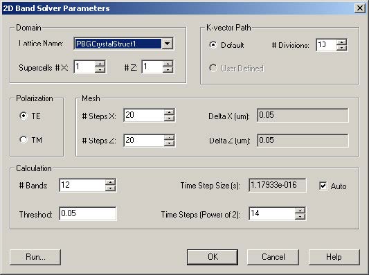
designer Simulation menu), OptiFDTD automatically checks to see if the lattice structure exists in the layout. Available lattice structures are listed under Domain, in the Lattice Name drop-down list. Currently only 2D square lattice and 2D hexagonal lattice are supported.
The FDTD simulation takes one unit cell as the fundamental periodic cell. You can specify how many unit cells are to be used for the simulation under Domain. This is controlled by Supercells #X (in x -direction) and #Z (in z-direction). Usually a 1×1 cell (unit cell) is good enough for extracting the band diagram.
You can also specify the TE or TM wave under Polarization.
When you specify the supercell, you then need to set the mesh size for the FDTD
simulation, in Mesh.
The FDTD simulation finds the eigen modes for one given K-vector. The K-vectors (a series value) are defined under K-vector Path. The Division number refers to how many K-vector sampling points there are for each sub-K-vector path. Please refer to the Technical Background to see how we set the default K-path.
The FDTD band solver calculation is controlled by four items, other than the mesh:
- # Bands—the number of modes extracted from the FDTD simulation.
- Threshold—the eigen value is obtained from the spectrum response which the peak value is normalized to unit. If sub-peak value is smaller than this threshold value, then the value is not regarded as a mode.
- Time Step Size (s)—domain size, time interval for FDTD simulation.
- Time Steps (Power of 2)—FFT is used to get the spectrum response. The FDTD simulation needs to run for 2N time steps to match the FFT requirement. So the value of N should be specified.
Setting the band solver simulation parameters
| Step | Action |
| 1 | From the Simulation menu, select 2D Band Solver Parameters.
The 2D Band Solver Parameters dialog box appears (see Figure 30). |
| 2 | Type/select the following information: Lattice Name: PBGCrystalStruc1
Supercells: #X: 1 #Z: 1 K-vector Path: # Divisions: 10 Polarization: TE Mesh: # Steps X: 20 # Steps Z: 20 Calculation: # of Bands: 12 Threshold: 0.05 Time Step Size [s]: Auto Time Steps [Power of 2]: 14 |
| 3 | Type/select the following information:
Lattice Name: PBGCrystalStruc1 Supercells: #X: 1 #Z: 1 K-vector Path: # Divisions: 10 Polarization: TE Mesh: # Steps X: 20 # Steps Z: 20 Calculation: # of Bands: 12 Threshold: 0.05 Time Step Size [s]: Auto Time Steps [Power of 2]: 14 |
Figure 30: 2D Band Solver Parameters dialog box
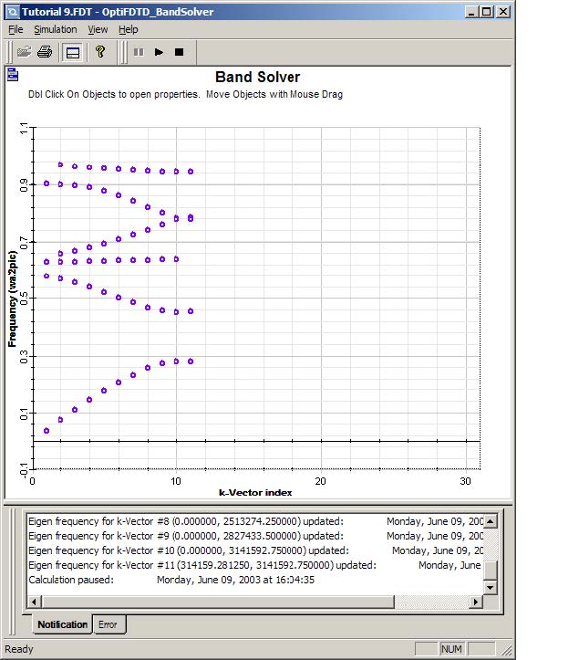
The band diagram is updated instantaneously for each K-vector value. The corresponding K-vector value is shown in the output box at the bottom of the OptiFDTD_BandSolver dialog box.
Figure 31: OptiFDTD_BandSolver
When the simulation is finished, the results are saved to a file with a *.bnd extension.
Viewing the simulation results
| Step | Action |
| 1 | In the OptiFDTD_BandSolver, select File > Load results.
The Select 2D Band Solver Result File dialog box appears. |
| 2 | Select the *.bnd file that you want to view and click Open.
The results are displayed in the OptiFDTD_BandSolver dialog box. |


