Using the same layout created in 2D-TE plane wave in unique material, create another file with the same layout by selecting File > Save As and using a different file name.
| Step | Action |
| 1 | From the Edit menu, select Wafer Properties.
The Wafer Properties dialog box appears. |
| 2 | Click the 3D Wafer Properties tab and set the Cladding: Material and Substrate Material to N=2. |
| 3 | Click OK.
The Wafer Properties dialog box closes. |
| 4 | To edit the input plane, double-click on the input plane in the layout.
The Input Plane Properties dialog box appears. |
| 5 | On the General tab, type/select the following:
Continuous Wave Wavelength [μm]: 2.0 Input Field Transverse: Rectangular Plane Geometry: Z Position [μm]: 1.0 |
| 6 | On the 3D Transverse tab, type/select the following:
Center Position [μm] X: 0.0 Halfwidth [μm] X: 5.0 Center Position [μm] Y: 0.0 Halfwidth [μm] Y: 5.0 Tilting Angle [deg]: 0 Effective Refractive Index: Local Polarization: LinearY Select the Amplitude radio button and type: Amplitude [V/m2]: 1.0 |
| 7 | Click OK.
The Input Field Properties dialog box closes. |
Setting the 3D-Y-direction polarized plane wave simulation parameters
| Step | Action |
| 1 | From the Simulation menu, select 3D Simulation Parameters.
The 3D Simulation Parameters dialog box appears. |
| 2 | Type/select the following information:
Mesh Delta X [μm]: 0.1 Mesh Delta Y [μm]: 0.1 Mesh Delta Z [μm]: 0.1 |
| 3 | Click Advanced….
The Boundary Conditions dialog box appears. -X: PMC +X: PMC -Y: PEC +Y: PEC -Z: Anisotropic PML +Z: Anisotropic PML Anisotropic PML Calculation Parameters Number of Anisotropic PML Layers: 10 Theoretical Reflection Coefficient: 1.0e-12 Real Anisotropic PML Tensor Parameters: 1.0 Power of Grading Polynomial: 3.5 |
| 4 | Click OK.
The Boundary Conditions dialog box closes. |
| 5 | In Time Parameters, click Calculate.
The default time step size is calculated. |
| 6 | Select Run for 1000 Time Steps (Results Finalized). |
| 7 | Select Key Input Information: Input Plane1 and wavelength:2.00. |
| 8 | Select DFT Options: Electric Components: Ey. |
| 9 | Click Run to start the OptiFDTD Simulator. |
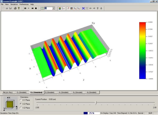
When the simulation is running, the plane wave effect can be observed in the
simulator (see Figure 26).
Figure 26: 3D Y-direction polarized plane wave


