Creating a layout
| Step | Action |
| 1 | Open the Waveguide Layout Designer. |
| 2 | To create a new project, select File > New.
The Initial Properties dialog box appears. |
| 3 | Click Profiles and Materials.
The Profile Designer window appears. |
| 4 | Under the Materials folder, right-click the Dielectric folder and select New.
A new Dielectric material dialog box appears. |
| 5 | Type the following information: Name: N=2
Refractive index (Re:): 2.0 |
| 6 | To save the material, click Store.
N=2 appears in the Dielectric folder in the directory and in the dialog box title bar. |
Defining the channel profile
| Step | Action1 |
| Under the Profiles folder, right-click the Channel folder and select New.
The ChannelPro1 dialog box appears. |
|
| 2 | Create the following channel profile: Profile name:
Profile_n=2 2D profile definition Material: N=2 3D profile definition Layer name: layer_01 Width: 1.0 Thickness: 1.0 Offset: 0.0 Material: N=2 Click Add. |
| 3 | Click Store. |
| 4 | Close the Profile Designer. |
Defining wafer and waveguide properties
| Step | Action |
| 1 | In the Initial Properties dialog box, type/select the following:
Waveguide Properties Width [μm]: 1.0 Profile: Profile_n=2 Wafer Dimensions Length [μm]: 8.0 Width [μm]: 4.0 2D Wafer Properties Material: Air 3D Wafer Properties Cladding Thickness [μm]: 2.0 Material: Air Substrate Thickness [μm]: 2.0 Material: Air |
| 2 | Click OK.
The Initial Properties dialog box closes. |
Inserting the input plane
To insert the input plane, perform the following procedure.
| Step | Action |
| 1 | From the Draw menu, select Vertical Input Plane. |
| 2 | To insert the input plane, click in the layout window where you want it placed.
The input plane appears in the layout. |
| 3 | To edit the input plane, double-click on the input plane in the layout.
The Input Plane Properties dialog box appears. |
| 4 | On the General tab, type/select the following:
Continuous Wave Wavelength [μm]: 1.55 Input Field Transverse: Rectangular Plane Geometry: Z Position [μm]: 1.0 |
| 5 | On the 2D Transverse tab, type/select the following:
Center Position [μm]: 0.0 Halfwidth [μm]: 5.0 Tilting Angle [deg]: 0 Effective Refractive Index: Local Amplitude [V/m]: 1.0 |
| 6 | Click OK.
The Input Field Properties dialog box closes. |
Setting the 2D TE FDTD simulation parameters
| Step | Action |
| 1 | From the Simulation menu, select 2D Simulation Parameters.
The Simulation Parameters dialog box appears. |
| 2 | Type/select the following information:
Polarization: TE Mesh Delta X [μm]: 0.05 Mesh Delta Z [μm]: 0.05 |
| 3 | Click Advanced….
The Boundary Conditions dialog box appears. -X: PMC +X: PMC -Z: Anisotropic PML +Z: Anisotropic PML Anisotropic PML Calculation Parameters Number of Anisotropic PML Layers: 10 Theoretical Reflection Coefficient: 1.0e-12 Real Anisotropic PML Tensor Parameters: 5.0 Power of Grading Polynomial: 3.5 |
| 4 | Click OK.
The Boundary Conditions dialog box closes. |
| 5 | In Time Parameters, click Calculate.
The default time step size is calculated. |
| 6 | Select Run for 1000 Time Steps (Results Finalized). |
| 7 | Select Key Input Information: Input Plane1 and wavelength:1.55. |
| 8 | Click OK to close the Simulation Parameters dialog box without running the simulation, or click Run to start the OptiFDTD Simulator. |
Running the 2D TE plane wave simulation
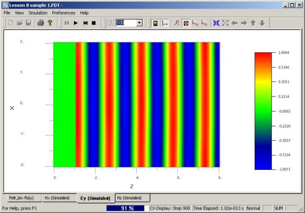
When you start the simulation, the plane wave propagation can be observed
(see Figure 25).
Figure 25: OptiFDTD Simulator


