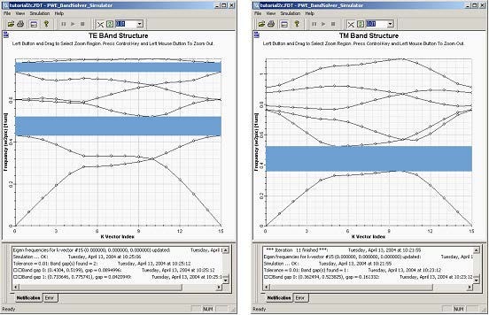
We are now going to verify band structure of 2D hexagonal lattice as reported in reference [1]. At this point you might want to save the current file under different name. The photonic structure we want to analyze consists of a hexagonal pattern of air holes in dielectric with permittivity 13. We have defined all the necessary materials and profiles at the beginning of this tutorial so the transition is easy.
To change the layout double click on the lattice to open Crystal Lattice Properties dialog. Change the lattice type from 2D Rectangular to 2D Hexagonal. Then Edit the properties of the elliptic waveguides (lattice atom waveguide). Change the minor and major radius from 0.2a to 0.48a and the profile to Chan_eps1. The last thing is to change the substrate from air to dielectric material eps13 (Edit >> Wafer Properties…>> 2D Wafer Properties) and check the index distribution in the 2D Refractive Index View.
Before running simulation we want to change the Simulation parameters of the PWE band solver, to get desired polarization, number of bands, and mainly to set up correct k-path.
In the PWE Parameters dialog uncheck the Inversion Symmetry, select TE polarization, use defaults for lattice vectors and mesh (16×16). Make sure the Domain Origin is set to (0,0,0). Set Number of Bands to 6 and tolerance to 10-5. In the K- vector Path select the predefined HexagonalZX option. The definition of the Brillouin zone can be found in the Technical Background.
Run the simulation to obtain the results for TE and TM. Keep the results for further comparison. Now increase the mesh resolution to 32×32. Also notice that the structure has an inversion symmetry so you might check the Inversion symmetry check box. Run the simulation with new parameters and compare the results with the first simulations. Even though the structures might look similar you will notice a difference in band gaps. This is due to the rough discretization, which cannot make details of the layouts. The air occupies most of the unit cell with filling factor of 0.836.
Figure 4: Band Diagram for Hexagonal Lattice


