OptiFDTD provides four types of nonlinear materials.
- 2nd Order
- 3rd Order
- Kerr-effect
- Raman-effect
All of these nonlinearities can be combined with the Lorentz dispersive model, which leads to dispersive nonlinear properties. To simulate the nonlinear material correctly, we recommend that you read the FDTD Basics.
Note:
- Because the nonlinear material may have a high frequency response, a finer mesh size for the simulation may be required.
- Set a suitable power level in the input plane. If the input power is too low, the material may not be excited to nonlinear levels. If the power is too high, the output will be an unstable modulated wave.
- Nonlinear material parameters must have physical meanings.
The following examples explain how to design, simulate, and analyze the nonlinear materials.
2nd Order nonlinear material simulation
Creating the layout
| Step | Action |
| 1 | Start Waveguide Layout Designer. |
| 2 | To create a new project, select File > New. The Initial Properties dialog box appears. |
| 3 | Click Profiles and Materials. The Profile Designer window appears. |
| 4 | Under the Materials folder, right-click the FDTD-Nonlinear folder and select New. A new FDTDNonlinear1 material dialog box appears. |
| 5 | Select 2nd order. The 2nd order tab appears in the dialog box. |
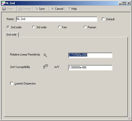
| 6 | Select/type the following: Name: NL 2nd Relative Linear Permittivity εL : 2.7225 2nd Susceptibility x( 2 ) m ⁄ V : 1.0e-6 |
| 7 | To save the material, click Store. |
Figure 8: FDTDNonlinear1 material definition dialog box
| 8 | Under the Materials folder, right-click the Dielectric folder and select New. A new FDTDDielectric1 material dialog box appears. |
| 9 | Select/type the following information: Name: Dielectric_1.65 Const Ref. Idx N Re: 1.65 |
| 10 | To save the material, click Store. Dielectric_1.65 appears in the Dielectric folder in the directory and in the dialog box title bar. |
To define the channel profile, perform the following procedure.
| Step | Action |
| 1 | Under the Profiles folder, right-click the Channel folder and select New. The ChannelPro1 dialog box appears. |
| 2 | Create the following channel profile: Profile name: NL 2nd_1 2D profile definition Material: NL 2nd |
| 3 | Click Store. |
| 4 | Create a second profile: Profile name: Dielectric 1.65_1 2D profile definition Material: Dielectric 1.65 |
| 5 | Click Store. |
| 6 | Close the Profile Designer. |
To define the wafer and waveguide properties, perform the following procedure.
| Step | Action |
| 1 | In the Initial Properties dialog box, type/select the following: Waveguide Properties Width [μm]: 1.0 Profile: NL 2nd_1 Wafer Dimensions Length [μm]: 10.0 Width [μm]: 5.0 2D Wafer Properties Material: Air |
| 2 | Click OK. The Initial Properties dialog box closes and the layout window appears. |
To create the waveguide, perform the following procedure.
| Step | Action |
| 1 | From the Draw menu, select Linear Waveguide. |
| 2 | In the layout window, drag the linear waveguide from the start point to the end point. A linear waveguide appears in the layout window. |
| 3 | To adjust the position and the shape of the waveguide, in the layout window, double-click the Linear Waveguide. The Linear Waveguide Properties dialog box appears. |
| 4 | Click the Start tab. |
| 5 | Under Offset, type the following values: Horizontal: 3 Vertical: 0 |
| 6 | Click the End tab. |
| 7 | Under Offset, type the following values: Horizontal (µm): 10.0 Vertical (µm): 0.0 |
| 8 | In Channel Thickness Tapering, select Use Default (Channel:None). |
| 9 | Type/select the following: Width (µm): 1.0 Depth (µm): 0.0 Label: Linear2 Profile: NL 2nd_1 |
| 10 | Repeat steps [1] through [9] to create another linear waveguide in the layout. |
| Step | Action |
| 1 | In Start > Offset, type the following values. Horizontal: 0 Vertical: 0 |
| 2 | In End > Offset, type the following values: Horizontal: 3 Vertical: 0 |
| 3 | Type/select the following: Width (µm): 1.0 Depth (µm): 0.0 Label: Linear1 Profile: Dielectric 1.65_1 |
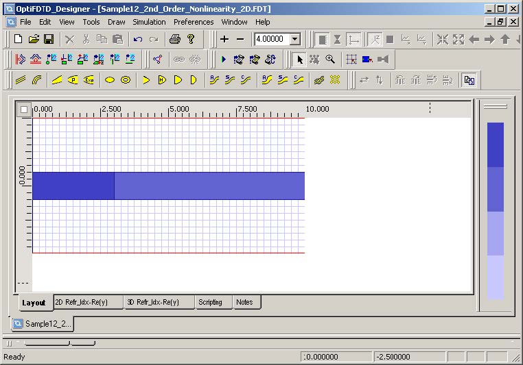
The two waveguides appear in the layout. The one on the left is the linear waveguide,
and the one on the right is the nonlinear waveguide (see Figure 9).
Figure 9: Waveguides in layout
Inserting the input plane
To insert the input plane, perform the following procedure.
| Step | Action |
| 1 | From the Draw menu, select Vertical Input Plane. |
| 2 | To insert the input plane, click in the layout window where you want it placed. The input plane appears in the layout. |
| 3 | To edit the input plane, double-click on the input plane in the layout. The Input Plane Properties dialog box appears. |
| 4 | Select Continuous Wave. |
| 5 | Set Wavelength to 1.5 μm. |
| 6 | On the General tab, type/select the following: Input Field Transverse: Modal Plane Geometry Z Position [μm]: 1.25 Positive direction |
| 7 | On the 2D Transverse tab, click Find Modes. The Mode Solver 2D dialog box appears. |
| 8 | On the Waveguides tab, select Linear1. |
| 9 | Click Calculate Mode. The Modes tab is activated. |
| 10 | On the Modes tab, select the mode. |
| 11 | Click Apply Data. The Mode Solver 2D closes. |
| 12 | On the 2D Transverse tab, select the Power radio button, and type the following: Power [W/m]: 16.0 |
| 13 | Click OK. The Input Field Properties dialog box closes. |
Setting up the Observation Point
| Step | Action |
| 1 | From the Draw menu, select Observation Point. |
| 2 | Place the Observation Point in the desired position in the layout. |
| 3 | Double-click the observation point. The Observation Properties — Point dialog box appears. |
| 4 | On the General tab: In Center, Offset, type/select the following: Horizontal: 2.5μm Vertical: 0.0μm Center depth: 0.0μm Label: ObservationPoint1 |
| 5 | On the Data Components tab, ensure that 2D TE: Ey is selected (default). |
| 6 | Click OK. The Observation Properties — Point dialog box closes. Repeat steps 1 to 5 to create the following additional observation points with the following information: On the General tab: In Center, Offset, type/select the following: Horizontal: 4.5μm Vertical: 0.0μm Center depth: 0.0μm Label: ObservationPoint2 Click OK. On the General tab: In Center, Offset, type/select the following: Horizontal: 6.0μm Vertical: 0.0μm Center depth: 0.0μm Label: ObservationPoint3 Click OK. On the General tab: In Center, Offset, type/select the following: Horizontal: 7.4μm Vertical: 0.0μm Center depth: 0.0μm Label: ObservationPoint4 Click OK. On the General tab: In Center, Offset, type/select the following: Horizontal: 9.0μm Vertical: 0.0μm Center depth: 0.0μm Label: ObservationPoint5 Click OK. On the General tab: In Center, Offset, type/select the following: Horizontal: 0.625μm Vertical: 0.0μm Center depth: 0.0μm Label: ObservationPoint6 Click OK. |
Setting the observation area
| Step | Action |
| 1 | From the Draw menu, select Observation XZ. |
| 2 | Place the Observation Area in the desired position in the layout. |
| 3 | Double-click the observation area. The Observation Properties — XZ Area dialog box appears. |
| 4 | On the General tab: In Center, Offset, type/select the following: Horizontal: 3.0μm Vertical: 0.0μm Center depth: 0.0μm Z length: + 1.5 X length: + 1.5 Label: ObservationArea1 |
| 5 | On the Data Components tab, select the following: 2D TE: Ey, Hx, Hz |
| 6 | Click OK. |
Setting the observation line
The observation line is only used for 2D simulations. It is used to show:
- field distribution along the line for the user input wavelength
- calculate the outgoing power in the line for user input wavelength
- calculate the absolute power spectrum and normalized transmittance power spectrum (to the input power)
| Step | Action |
| 1 | From the Draw menu, select Observation Vertical Line. |
| 2 | Place the Observation Line in the desired position in the layout. |
| 3 | Double-click the observation line. The Observation Properties — Vertical Line dialog box appears. |
| 4 | On the General tab: In Center, Offset, type/select the following: Horizontal: 9.5μm Vertical: 0.0μm X length: + 2.0 Label: ObservationLine1 |
| 5 | On the Data Components tab, select the following: 2D TE: Ey, Hx, Hz |
| 6 | Click OK. Repeat steps 1 to 5 to create an additional observation line with the following information: |
| 7 | On the General tab: In Center, Offset, type/select the following: Horizontal: 6.5μm Vertical: 0.0μm X length: + 2.0 Label: ObservationLine2 |
| 8 | On the Data Components tab, select the following: 2D TE: Ey, Hx |
| 9 | Click OK. |
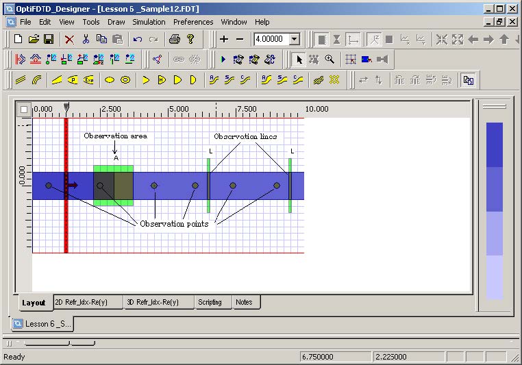
The observation components of the project can be seen in Figure 10.
Figure 10: Observation components of project
Setting the 2D simulation parameters
| Step | Action |
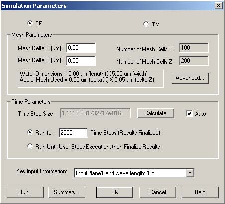
| 1 | From the Simulation menu, select 2D Simulation Parameters. The Simulation Parameters dialog box appears (see Figure 11). |
| 2 | Type/select the following information: Polarization: TE Mesh Delta X [μm]: 0.05 Mesh Delta Y [μm]: 0.05 |
Figure 11: Simulation Parameters dialog box
| 3 | Click Advanced…. The Boundary Conditions dialog box appears. |
| 4 | Type/select the following information: Anisotropic PML Calculation Parameters Number of Anisotropic PML Layers: 20 Theoretical Reflection Coefficient: 1.0e-12 Real Anisotropic PML Tensor Parameters: 5.0 Power of Grading Polynomial: 3.5 |
| 5 | In Time Parameters, click Calculate. The default time step size is calculated |
| 6 | Select Run for 2000 Time Steps (Results Finalized). |
| 7 | Select Key Input Information: Input Plane1 and wavelength:1.5. Note: The input plane’s center wavelength is used for DFT calculations. |
| 8 | Click OK to close the Simulation Parameters dialog box without running the simulation, or click Run to start the OptiFDTD Simulator. Note: Before running the simulation, save the project to a file. |
Observing the simulation results in OptiFDTD Simulator
Key things to observe:
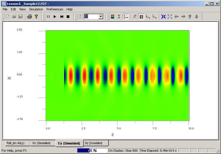
- Field propagation pattern in OptiFDTD Simulator (see Figure 12)
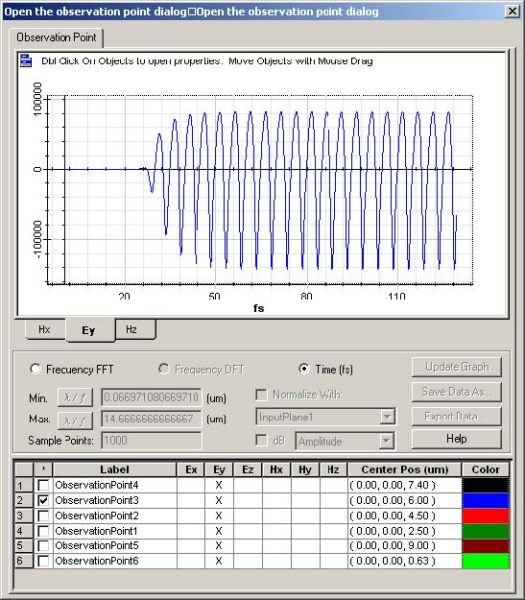
Select View > Observation Point to observe the dynamic time domain and frequency domain response (see Figure 13).
Figure 12: Field propagation pattern
Figure 13: Observation point
Performing data analysis
When the simulation ends, a message appears and prompts you to open
OptiFDTD_Analyzer (see Figure 23).
Figure 14: Message box
Action
- To open OptiFDTD_Analyzer and view the simulated results, click Yes.
Note: When the simulation ends in OptiFDTD_Simulator, the results are saved automatically as a file with same name, but with a different file extension (*.fda).
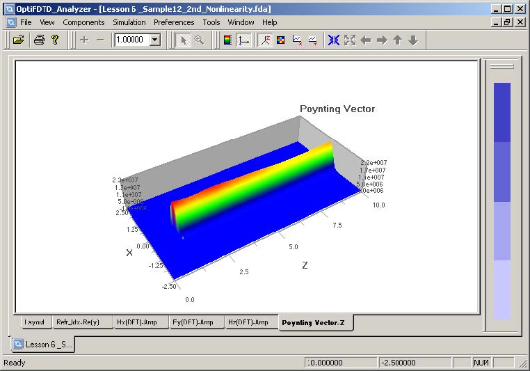
Observe the layout, refractive index, Poynting vector, and field propagation pattern (DFT results) for the input wavelength (see Figure 15 for Poynting vector in z-direction).
Figure 15: Poynting vector in z-direction
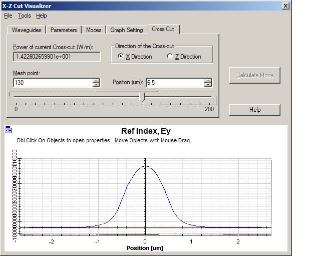
- Select Tools > Crosscut Viewer. The X-Z Cut Visualizer dialog box appears.
You can do the mode analysis, mode overlap integral calculation, slice power calculation, and far field transformation (see Figure 16).
Figure 16: X-Z Cut Visualizer
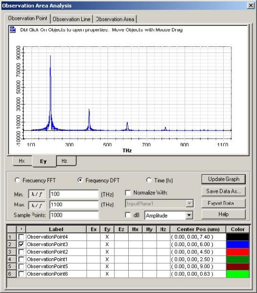
- Select Tools > Observation Area Analysis. The Observation Area Analysis dialog box appears (see Figure 17).
Figure 17: Observation Area Analysis dialog box
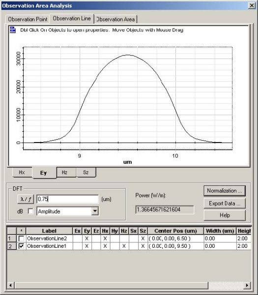
- Click the Observation Line tab to start the observation line analysis. The field pattern and the corresponding power for the user input wavelength in the observation line appear in the dialog box (see Figure 18).
Figure 18: Observation field pattern and power in observation line
You can also follow the same procedure to perform another nonlinear material simulation.
See the following sample files:
- Sample12_2D_TE_3rd_Order_Nonlinear.fdt
- Sample13_2D_TE_Kerr_Nonlinear.fdt
In general, the Kerr effect and Raman effect belong to the 3rd-order nonlinearity. However, the Kerr effect uses a special model to consider photonic response time, while the Raman model considers both the response time and the oscillating frequency.


