
| Step | Action |
| 1 | Open the OptiFDTD Waveguide Layout Designer. |
| 2 | To create a new project, select File > New. The Initial Properties dialog box appears. |
| 3 | Click Profiles and Materials. The Profile Designer window appears. |
| 4 | Under the Materials folder, right-click the Dielectric folder and select New. A new Dielectric material dialog box appears. |
| 5 | Type the following information: Name: er=8.9 Refractive index (Re:): 2.983287 |
| 6 | Click Store. |
Defining the channel profile
| Step | Action |
| 1 | Under the Profiles folder, right-click the Channel folder and select New. The ChannelPro1 dialog box appears. |
| 2 | Create the following channel profile: Profile name: Profile_PhC 2D profile definition Material: er=8.9 3D profile definition Layer name: layer_01 Width: 1.0 Thickness: 1.0 Offset: 0.0 Material: er=8.9 |
| 3 | Click Add. |
| 4 | Click Store. |
| 5 | Close the Profile Designer. |
Defining wafer and waveguide properties
| Step | Action |
| 1 | In the Initial Properties dialog box, type/select the following: Waveguide Properties Width [μm]: 1.0 Profile: Profile_PhC Wafer Dimensions Length [μm]: 10.0 Width [μm]: 10.0 2D Wafer Properties Material: Air 3D Wafer Properties Cladding Thickness [μm]: 1.0 Material: Air Substrate Thickness [μm]: 1.0 Material: Air |
| 2 | Click OK. The Initial Properties dialog box closes. |
Creating the PBG crystal structure
| Step | Action |
| 1 | From the Draw menu, select PBG Crystal Structure. |
| 2 | Click in the layout window to create the PBG area. The PBG Crystal Structure appears in the layout window. |
| 3 | Click on the Select tool. |
| 4 | To set the PBG properties, double-click on the PBG Crystal Structure in the layout. The Crystal Lattice Properties dialog box appears (see Figure 27). |
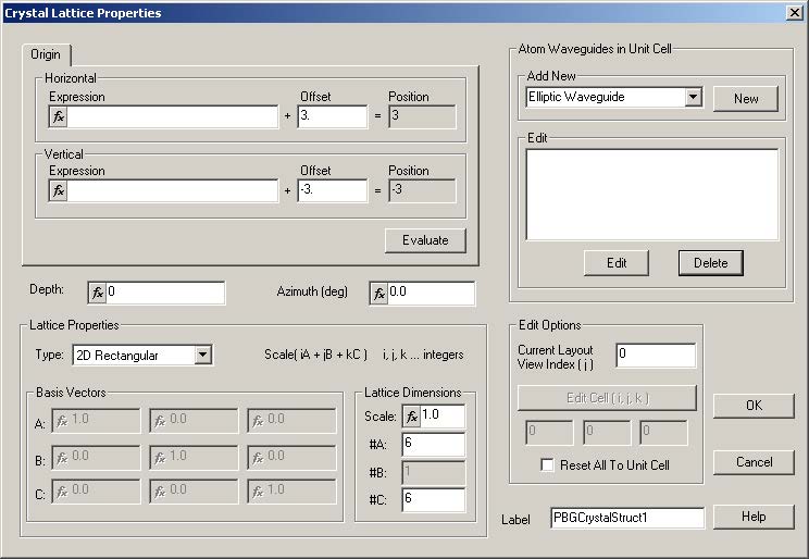
Figure 27: Crystal Lattice Properties dialog box
| 5 | In Origin, Offset, type/select the following: Horizontal: 3.0 Vertical: -3.0 |
| 6 | Click Evaluate. |
| 7 | Type/select the following: Depth: 0.0 Azimuth [deg]: 0.0 |
| 8 | In Lattice Properties, select Type: 2D Rectangular. |
| 9 | In Lattice Dimensions, type/select the following: Scale: 1.0 #A: 6 #C: 6 |
| 10 | In Label, type PBGCrystalStruct1. Note: Do NOT close the Crystal Lattice Properties dialog box. |
Setting the atom properties
To set the atom properties, perform the following procedure in the Crystal Lattice Properties dialog box.
| Step | Action |
| 1 | In Atom Waveguide in Unit Cell, Add New, select Elliptic Waveguide from the drop-down menu and click New. The Elliptic Waveguide Properties dialog box appears. |
| 2 | In Center, Offset, type/select the following: Horizontal: 0.0 Vertical: 0.0 |
| 3 | Type/select the following: Major radius: 0.2 Minor radius: 0.2 Orientation Angle: 0.0 Channel Thickness Tapering: Use Default (Channel: None) Depth: 0.0 Label: Atom Profile: Profile_PhC. |
| 4 | Click OK. The Elliptic Waveguide Properties dialog box closes. Note: When you return to the Crystal Lattice Properties dialog box, you will see the defined elliptic waveguide listed in Atom Waveguide in Unit Cell (see Figure 29). |
| 5 | Click OK in the Crystal Lattic Properties dialog box. |

Figure 28: Defined elliptic waveguide in Unit Cell Edit table

Figure 29: Defined PhC structure in layout