In this example, we will show how a gold particle is simulated by OptiFDTD. In some
surface Plasmon layouts, gold particles may distribute in an array format, if the input
plane wave propagate straight forward and the array is periodic, then we can take one
periodic cell for the simulation with transverse boundary set as periodic boundary
condition (PBC). If single gold particle works independently, we can either set
transverse boundary as absorbing condition or still set transverse boundary as PBC
with simulation space is two three time larger than the nanoparticle size.
The sample layout can be found in the 64bit sample folder, it is named as
“X64_Sample52_100nmGoldSphere_400nm_900nmPulse.fdt”
| Step | Action |
| 1 | Open OptiFDTD Waveguide layout Designer From the Start menu, select Programs –>Optiwave Software –> OptiFDTD-> Waveguide Layout Designer. OptiFDTD_Designer window opens. |
| 2 | Create a new project.
From the OptiFDTD_Designer File menu, select New. The Initial Properties dialog box appears. |
| 3 | Define the material(s) and waveguide profile(s) that will be used in the project. Click the Profiles and Materials button in the Initial Properties dialog. The Profile Designer OptiFDTD opens.
Note: At any time, you can open the Profile Designer from the “Edit->Profiles and Materials…” menu of the Layout Designer or from the Start menu. So you can make appropriate modifications to the defined materials and profiles whenever it is needed. a. In the material folder of Master. Find build in gold material “Gold_Au_Lorentz_Drude_Model”, select this material and drag it to FDTD-Dispersive folder under Materials folder of current project OptiFDTD_Designer1, Click Store button in the OptiFDTD_Designer1, Click Store button in the Gold_Au_Lorentz_Drude_Model dialog box to save this material to the project. b. In the directory under OptiFDTD_Designer1, under the Profiles folder, right click the Channel folder. A context menu appears. Select New. The Channel Profile dialog box appears. Type the following information: • Profile name: ChannelPro1 • Under 3D profile definition: Type the following information: Layer name: Layer1 Width: 0.1 Thickness: 0.1 Offset: 0.0
• In the Material list, select Gold_Au_Lorentz_Drude_Model • Click Add. • To save the channel profile, click Store. ChannelPro1 appears in the Channel folder. |
| 4 | Return to Initial Properties dialog box of Waveguide Layout Designer.
Either minimize or close the Waveguide Profile Designer. |
| 5 | Type the following information in each corresponding area in Initial Properties dialog box
• Waveguide Properties: Width ( μm ): 0.1 Profile: ChannelPro1 • Wafer Dimension Length ( μm ): 0.6 (z-direction dimension) Width ( μm ): 0.3 (x-direction dimension) • 3D Wafer Properties Cladding Material: Air Cladding Thickness: 0.3(y-direction dimension) Substrate Material: Air Substrate Thickness: 0 (y-direction dimension) |
| 6 | Click OK in Initial Properties dialog box. OptiFDTD Designer- [OptiFDTDigner1] window appears.
Note: • If not all Toolbars appear in the Layout Desinger window, you can change it from the “View-Toolbars” menu option. • Click “+” (zoom) toolbar button to enlarge the layout window. • Open “Wafer Properties” from the Edit menu to modify simulation domain properties. • Select “Profiles and Materials” from the Edit menu to open the Profile Designer where you can add and modify materials and profiles. |
| 7 | Draw a nano-particle in the layout.
• Select sphere under the 3D shapes of Draw menu. • Click the mouse in the layout where the particle should be put. • Click on the arrow shortcut icon in the toolbar to release the sphere from the 3D shapes selection. • To adjust the position and the shape of the waveguide, in the layout window,double-click the sphere. The Sphere Waveguide Properties dialog box appears • In the sphere waveguide properties dialog box, type the following values: Position x: 0 Position y: 0.15 (m) Position z: 0.35 (m) Radius: 0.05 (m) Lable: Sphere1 Material: Gold_Au_Lorentz_Drude_Model • Click OK to finished the sphere setting Note: You can parameterize the waveguide by entering a user-defined variable (parameter) in the Expression field. The expression fields are marked with “fx”. For example you can enter StartPosZ (or an expression like 2*StartPosZ), in the Expression field of Horizontal position definition. After that press the Evaluate button, to see the resulting Position value. If the specified parameter has not been defined, then the software will prompt you to define it. |
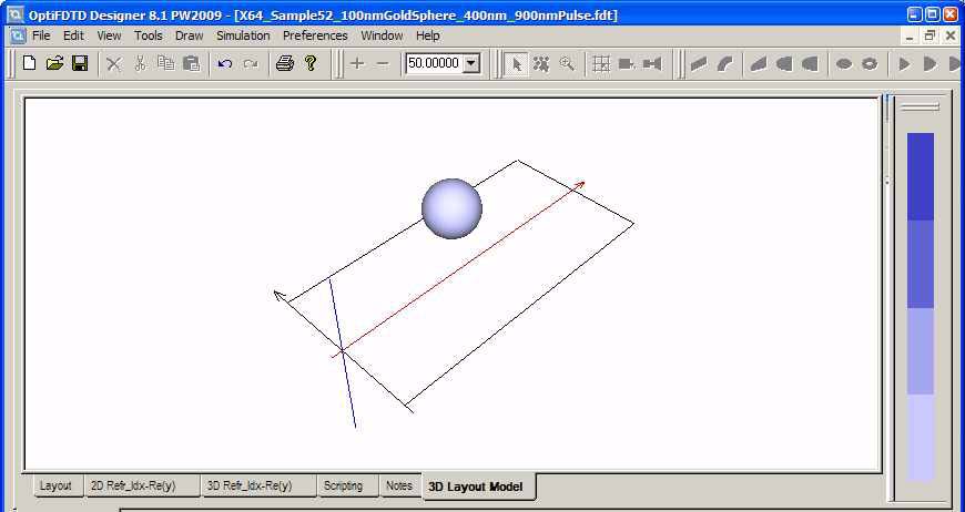
| 8 | Click 3D Layout Model tab under the layout window to observe the layout in 3D mode (see Figure 1) |
Figure 1: 3D layout mode for sphere
Define Input Wave
The Input Wave signal is defined within the Input Plane. To insert the Input Plane and
set the excitation wave, follow the steps below:
| Step | Action |
| 1 | From the Draw menu, select Vertical Input Plane, or select Vertical Input Plane shortcut toolbar (The Vertical Input Plane is in the x-y plane for 3D.) |
| 2 | Click in the layout window at the position where you want to insert the Input Plane. A red line that represents the input plane appears in the layout window. |
| 3 | To set up the Input Plane properties, double-click the red line (Input Plane) in the layout window. The Input Field Properties dialog box appears. |
| 4 | Set the time domain Input Plane basic information.
a. Select Gaussian Modulated Continuous Wave. The Gaussian Modulated CW tab appears. b. Wavelength ( μm ): 0.55( μm ) Note: • Continuous Wave: Wavelength is a single wavelength that is used in simulations. • Gaussian Modulated Continuous Wave: Wavelength is the carrier wavelength (center wavelength) for the pulse simulations. |
| 5 | Click the Gaussian Modulated CW tab to set the time domain input waveform. The time domain pulse graphics appear. Type the following values for the time domain input plane:
Time offset (sec.): 4.0e-15 Half width (sec.): 0.8e-15 Note: • Right Click on the graph and select the Zoom In tool to enlarge the selected graph region. You can observe the bandwidth in this way. • Adjust half width can adjust the bandwidth |
| 6 | To set up the general information (transverse field distribution) for the Input:
Plane, click the General tab Input Field Transverse: Rectangular( windowed plane wave) Z Position ( μm ): 0.2 Plane Geometry: Positive direction Label: InputPlane1 (default) |
| 7 | Click 3D Transverse to setup the plane wave setting
• Center Position X: 0.0(μm ); Halfwidth X: 0.2( μm ) • Center Position Y: 0.15 ( μm ); Halfwidth Y: 0.2( μm ) • Effective index: Local • Polarization: Linear Y • Amplitude: 1.0 (V/m2) To complete the Input plane setup, click OK. |
Define Simulation Parameters
| Step | Action |
| 1 | From the Simulation menu, select Simulate 3D Using 64-bit Simulator.
The 3D Simulation Parameters dialog box appears. |
| 2 | In the mesh size region deselect “Auto” boxes, type the following values for the mesh size:
Mesh Delta X (m): 0.004 Mesh Delta Y (m): 0.004 Mesh Delta Z (m): 0.004 |
| 3 | To set up the boundary condition parameters, click Advanced. The Boundary Conditions dialog box appears.
• Set X and Y direction boundary condition as PBC • Set Z direction boundary condition as APML • Type the following values for the PML boundary condition: Anisotropic PML layer number: 16 Theoretical Reflection Coefficient: 1.0e-12 Real Anisotropic PML Tensor Parameter: 60.0 Power of grading Polynomial: 3.5 |
| 4 | Run for 4000 time steps |
| 5 | Time sampling interval: 2
Note: • Time steps size The default value ensures stability and accuracy of FDTD simulations • Time step number The default value ensures that the wave completes propagation through the whole layout • Time sampling interval This sampling rate applies to observation areas. It determines how many time domain response sample points are used for the spectrum calculation. |
| 6 | Click the “Spectrum” button to set the spectrum range
• Set “Number of Samples” to 101, • Uncheck the “Auto” checkbox, • Check the “Use Wavelength” radio button • Set Start wavelength as 0.4 μm • Set end wavelength as 0.9 μm • and press Ok button to accept changes |
Setup the Observation Objects (result data-detector)
For the 32-Bit FDTD simulation, observation objects will record all the time domain response so that spectrum analysis can be performed in analyzer. For 64-Bit FDTD simulation, Observation points will still record all the time domain response in each single point, but Observation area will perform the spectral analysis in simulator and save the spectrum DFT results to the analyzer file. For 64bit FDTD simulation,
Observation Points or Observation Area must be present; otherwise simulations will not store any results for further analysis.
• Observation Point
Observes the time domain and frequency domain response. The transmission function can be obtained from the Observation Point analysis.
• Observation Area
It is used to compute power transmission ratio, and normalized power (power
transmission /reflection) versus wavelength.
| Step | Action |
| 1 | From the Draw menu (or the shortcut toolbar), select Observation XY Area. |
| 2 | Place the Observation XY Plane in the position after the sphere in the layout. |
| 3 | Double-click the observation XY Area. The “Observation Properties – X-Y Area” dialog box appears. Type the following values in the dialog box:
General Center Horizontal Offset (z-drection): 0.5( μm ) Center Vertical Offset(x-direction): 0.0(μm ) Center depth (y-direction): 0.15 ( μm ) X-Length 0.3 ( μm ) Y-Length 0.3 ( μm ) Label: ObservationArea1 Data Components Ex, Ey, Hx, Hy |
| 4 | Click OK to close the dialog box |
| 5 | Repeat steps 1 to 4 to design another Observation area with center horizontal offset at z=0.1 μm
General Center Horizontal Offset (z-drection): 0.1( μm ) Center Vertical Offset(x-direction): 0.0( μm ) Center depth (y-direction): 0.15 (m) X-Length 0.3 (m) Y-Length 0.3 (m) Label: ObservationArea2 μm ) Data Components Ex, Ey, Hx, Hy Note: Observation1 will get the power spectral transmission function, Observation 2 is behind input plane and it will get the power spectral reflection function. |
| 6 | In the same manner we can put observation point in the layout. |
Perform the 64Bit-FDTD Simulation
| Step | Action |
| 1 | From the Simulation menu, select the “Simulate 3D using 64-Bit Simulator…” option. The 3D Simulation Parameters dialog box appears. |
| 2 | Click Run to start the simulation. The progress window appears, it displays the status of the simulations. |
| 3 | Visualization of intermediate simulation results. configure the snapshot settings. In the calculation progress window, select “Simulation ->Take Snapshot” menu option. The “Set Snapshot” dialog box appears
• Click Browse to select the location of the output file • Check the observation areas or observation points. The time domain response in the selected observation objects for the current time-step will be save to the file • Click OK to close this dialog box |
| 4 | Click the “Take Snapshot” button in the simulation progress dialog box to save the time domain response in the current displayed time step |
| 5 | Go to the folder where the snapshot is saved and with 2D or 3D Viewer observe the time domain response for a certain time step |
When the simulation is finished, you will be asked if you want to open the analyzer to view the results. Click yes to start the analyzer view the results.
Post-Simulation Data Analysis
| Step | Action |
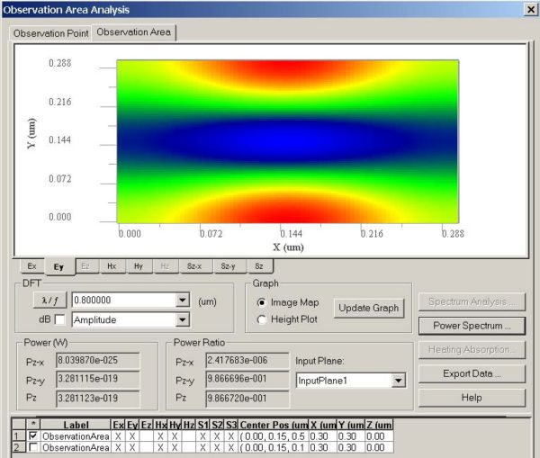
| 1 | Select “Observation Area Analysis” under the “Tools” menu in the Analyzer.
Select Observation area button to active observation area analysis, Observation Area dialog box appears |
| 2 | Select “ObservationArea1” in the observation area check list |
| 3 | Select Ey component. |
| 4 | Select wavelength 0.8 from the λ ⁄ f list box |
| 5 | Click Update Graph |
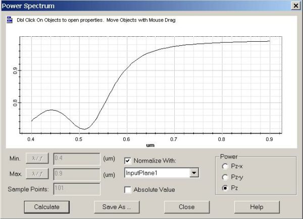
| 6 | Select Power Spectrum button, Power Spectrum dialog box appears, Select total Power “Pz”, Check “normalize with” checkbox and click Calculate button, Power Transmission spectrum appears. |
Figure 2: field pattern in observation area.
Figure 3: Power transmission function


