Scattering data is a new simulation feature in OptiBPM. OptiBPM uses scattering data when a small part of a larger photonic circuit is isolated for characterization using BPM. This smaller part has waveguides entering on the left side and exiting on the right side. The N inputs and the M outputs are assumed to have light in a modal configuration, although the input and output waveguides may be tilted.
You can export the scattering data matrix that OptiBPM produces to OptiSystem for future analysis.
This lesson describes how to generate and export scattering data and the connection between OptiBPM and OptiSystem simulators on a simple 2D directional coupler. There are two sections:
- Part I — OptiBPM
- Part II — OptiSystem
Before you start this lesson
- Complete Lesson 6: Design a 3dB coupler using VB Script.
Theoretical Background
We will analyze one of basic photonic circuits, the Mach-Zehnder Interferometer (MZI) shown in Figure 1 . The device actually consists of four basic components/devices and our goal is to divide the circuit into these primitive self-existing devices, or, in other words, the 3dB coupler. They can be separately simulated by means of OptiBPM and later analyzed as the entire device by OptiSystem.The device can be quite large, and therefore, consume an extended simulation time. Any division to a subcomponent decreases the time consumption drastically, because the simulation speed is proportional to the area of the component (see Scattering Data in the Technical Background for more information). At this point, we should emphasise the circuit division criteria are case sensitive and the decision is dependent on the user’s knowledge and experience, however the subcomponents (i.e. their boundaries ) are often visible naturally. On the other hand, an improper subcomponental division can cause false results. Moreover, the designer has already the principle of a given circuit operation clearly in mind prior to enitiating any practical design. In this example, we will design the MZI to have a maximum intensity for one wavelength and the minimum intensity (in the same port) for another wavelength. This is the principal behaviour of the MZI and it can be exploited as a basic switch, because the other output port obviously behaves in a complementary fashion to the first one.
The functionality of the device is well known. The light is launched into one input (we will select the upper input waveguide, marked ‘input’). The input 3dB coupler splits the light into two equal parts. The 3dB coupler was previously optimised to split the light equally from one input port to the output ones. The light then propagates independently through each arm. One of them is optically longer, what causes a phase difference at the ends of these arms. This can be achieved in several ways, we simply demonstrate this effect by increasing the core refractive index of the lower arm. Finally, the light coming from both arms enters the output coupler, which recombines the light depending on a magnitude of the phase difference. If there was no phase difference, the light should ideally appear just in the lower (‘B’) ouput port. However, with the presence of a certain phase difference, the light distribution will vary with changing wavelength. We will omit any theory here for the sake of brevity (you should refer to any basic photonic literature, such as [1]). Since we are interested of the wavelength dependence on the device bahaviour, the optical phase difference takes the form:

where λ is the wavelength, L is the arms length, n, (λ) and n2, (λ) are the effective indices of the upper and lower arm, respectively. The length of the arms in between the couplers is 3 mm. Regarding the material configurations, the core refractive index is 1.5, the cladding is 1.49 for all devices. The core refractive index of the lower arm is increased to the value 1.52. The width of all particular waveguides is 4 microns. A basic inspection of the effective indices shows, we should thus be interested to analyze the wavelength interval from1.534 nm to 1.554 nm to reach desired behaviour of the device (including couplers).
Obviously, we can see the following subcomponents in our case (see Figure 1):
- the input coupler
- the output coupler
- the two arms connecting the coupler
One (the lower) of the arms causes the desired phase difference Φ.
Figure 1: Schematics of MZI
Part I — OptiBPM
This section describes the procedures required to generate scattering data in OptiBPM. The procedures are:
- Generating Scattering Data script
- Exporting scattering data
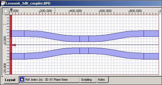
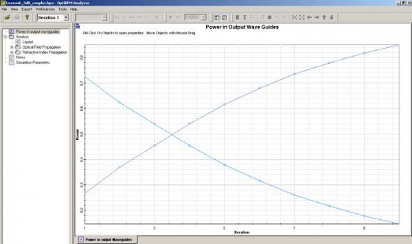
To start designing the 3dB coupler, we will use the coupler created in Lesson 6, where the influence of the distance between the coupling parts of the coupler was studied by a script (see Figure 2). When you run the sample file, you can see the the optimal half splitting power appearing somewhere between the 3rd and 4th iteration step (see Figure 3).
Figure 2: Lesson6_3db_coupler layout
Figure 3: Power in output waveguides — Lesson 6
To use the data in Lesson 6 to generate scattering data, perform the following procedure.
| Step | Action |
| 1 | Open the Lesson6_3dB_coupler.BPD file (see Figure ). For more information on creating this file, see Lesson 6: Design a 3dB coupler using VB Script.
Note: You can use any complete 2D layout (including input modal field) to generate scattering data. |
| 2 | Click the Scripting tab in the layout window. |
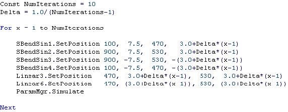
We will derive the coordinates of the waveguides in the coupler from the script code in Lesson 6. The end of the script code in Lesson 6 is:
It is obvious the vertical positions of the all SBends and the short central linear waveguides (Linear6 and Linear3) have to be defined accordingly. Considering the ideal coupling for x = 3.5 , the expressions from the script yield for the desired vertical positions the value 3.278 and -3.278, respectively. However, let us consider a slightly non-symmetric coupling (approximately 45% and 55% of the total power to each waveguide) as a fictitious simulation of an inaccurate fabrication. We will decrease the values slightly, to +/- 3.19. The easiest way to modify these vertical waveguides is to simply modify manually the pertinent waveguide coordinates. The coupler is saved as deriv_3dB.bpd for further exploitation.
To modify the waveguide properties for this lesson, perform the following procedure.
| Step | Action |
| 1 | Open the Lesson6_3dB_coupler.BPD file. For more information on creating this file, see Lesson 6: Design a 3dB coupler using VB Script. Note: You can use any complete 2D layout (including input modal field) to generate scattering data. |
| 2 | Double-click on the horizontal waveguide labeled Linear3 (see Figure 4) to open the Linear Waveguide Properties dialog box. |
| 3 | On the Start tab, type 3.19 in Vertical Offset. |
| 4 | On the End tab, type 3.19 in Vertical Offset. |
| 5 | Click OK.
The Linear Waveguide Properties dialog box closes. |
| 6 | Double-click on the horizontal waveguide labeled Linear6 (see Figure 4) to open the Linear Waveguide Properties dialog box. |
| 7 | On the Start tab, type -3.19 in Vertical Offset. |
| 8 | On the End tab, type -3.19 in Vertical Offset. |
| 9 | Click OK. The Linear Waveguide Properties dialog box closes. |
The ends of the S-bend waveguides must also be modified to meet the ends of Linear3 and Linear6.
| Step | Action |
| 1 | Double-click on the S-bend waveguide labeled SBendSin1 (see Figure 4) to open the S-Bend Sine Properties dialog box. |
| 2 | On the End tab, type 3.19 in Vertical Offset. |
| 3 | Click OK. The S-Bend Sine Properties dialog box closes. |
| 4 | Double-click on the S-bend waveguide labeled SBendSin2 (see Figure 4) to open the S-Bend Sine Properties dialog box. |
| 5 | On the End tab, type 3.19 in Vertical Offset. |
| 6 | Click OK. The S-Bend Sine Properties dialog box closes. |
| 7 | Double-click on the S-bend waveguide labeled SBendSin3 (see Figure 4) to open the S-Bend Sine Properties dialog box. |
| 8 | On the End tab, type -3.19 in Vertical Offset. |
| 9 | Click OK. The S-Bend Sine Properties dialog box closes. |
| 10 | Double-click on the S-bend waveguide labeled SBendSin4 (see Figure 4) to open the S-Bend Sine Properties dialog box. |
| 11 | On the End tab, type -3.19 in Vertical Offset. |
| 12 | Click OK. The S-Bend Sine Properties dialog box closes. |
| 13 | Save Lesson 6 with the new name, deriv_3dB.bpd. |
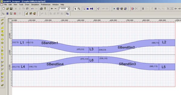
Note: Values in Figure 4 for Vertical Offset are shown as ±3.0 |- you change these to ±3.19.
Figure 4: Lesson6_3db_coupler.BPD file
Generating Scattering Data script
To generate the scattering data script, perform the following procedure.
| Step | Action |
| 1 | From the Simulation menu, select Generate Scattering Data Script or Click the Scattering Data Script button. 
A message box opens and informs you that the scattering data script will overwrite the current script (see Figure 5). |
Figure 5: Scattering data script message box
| 2 | Click Yes. The Scattering Data Scripting dialog box appears. |
| 3 | From the Input Plane drop-down list, select InputPlane1 (refer to Figure 6). |
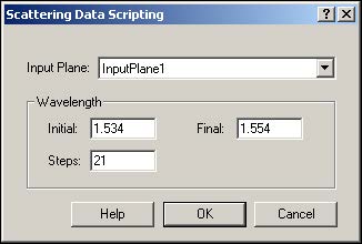
| 4 | To determine the scanning interval and the number of steps in the interval, type the following wavelength values: Initial: 1.534 Final: 1.554 Steps: 21 |
Note: The default number of steps is 3. When you select only one step, the results are wavelength-independent for further analysis.
Figure 6: Scattering Data Scripting dialog box
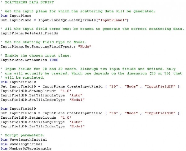
| 5 | Click OK. The Scripting window opens and displays the generated scattering data script (see Figure 7). |
Figure 7: Scripting window—Scattering data script
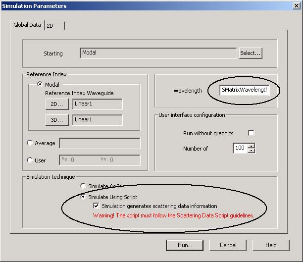
| 6 | From the Simulation menu, select Calculate 2D Isotropic Simulation. The Simulation Parameters dialog box appears (see Figure 8). Note: Under Simulation technique, Simulate Using Script and the Simulation generates scattering data information check box are selected automatically. SMatrixWavelength appears in the Wavelength box automatically, instead of a numerical value—the wavelength interval was set in Step 4. |
| 7 | Click the 2D tab and ensure that the correct simulation parameters are set. |
Figure 8: Simulation Parameters dialog box
| 8 | Click Run. OptiBPM_Simulator opens and the simulation runs. |
| 9 | When the simulation is complete, open OptiBPM_Analyzer to view the results. |
Exporting scattering data
There are two possibilities for the S-data export:
- Scattering Data in Cartesian Coordinates (exports √Pcos(Φ); √Psin(Φ) for each waveguide)
- Scattering Data in Polar Coordinates (exports √P;Φ for each waveguide).
Obviously, both are mathematically equal. However, the polar coordinates export is advantageous for relatively longer devices, because of further interpolation of slowly varying cumulative phase in OptiSystem. Therefore, only a few iteration steps are required. On the other hand, the Cartesian coordinates export is worth using in cases of sudden phase changes in the device behaviour, but quite a number of iterations is needed (i.e., frequently oscillating function is to be fitted in most cases).
To export the scattering data from OptiBPM_Analyzer to OptiSystem, perform the following procedure.
| Step | Action |
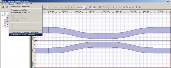
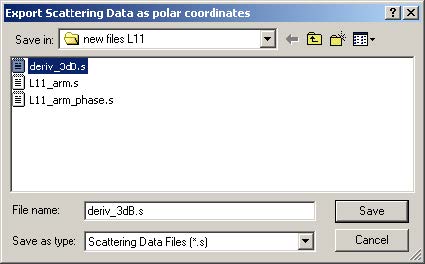
| 1 | From the Export menu, select Scattering Data in Polar Coordinates (see Figure 9). The Export Scattering Data dialog box appears (see Figure 10). |
| 2 | Save the data as an *.s file. |
Figure 9: Export menu—Scattering Data
Figure 10: Export Scattering Data dialog box
The procedure to generate and export scattering data is complete. The next procedure describes how to generate, use, and analyze the scattering data *.s file with OptiSystem.
Creating the arms
The layout consists of the straight linear waveguide. Use the following parameters:
Wafer size: 3000 x 30 μm
Waveguide width: 4
Waveguide length: 3 mm
Refractive index of the cladding: 1.49
Refractive index of the core (upper arm): 1.50
Refractive index of the core (lower arm): 1.52
Scan the wavelength with:
Initial: 1.534
Final: 1.554
Steps: 14
Note: Since we are dealing with the single straight waveguide, 14 or less steps should be accurate enough for the data export.
Following the procedure outlined for the 4 port coupler, generate the Sdata files for both arms (L11_Arm.bpd and L11_Arm.s; L11_Arm_phase.bpd and L11_Arm_phase.s, the latter one having a higher core refractive index).
Figure 11: The layout of the arms of MZI
Part II — OptiSystem
This section describes how to analyze the scattering data *.s file generated from OptiBPM in OptiSystem. The procedures are:
- Loading the *.s file in OptiSystem
- Loading the files for both Arms
- Completing the layout in OptiSystem
- Connecting the components
- Running the calculation
- Creating the graph to view the results
Loading the *.s file in OptiSystem
To load the *.s file into the OptiBPM Component NxM in OptiSystem, perform the following procedure.
| Step | Action |
| 1 | From the Start menu on the task bar, select Programs > Optiwave Software > OptiSystem > OptiSystem. OptiSystem opens. |
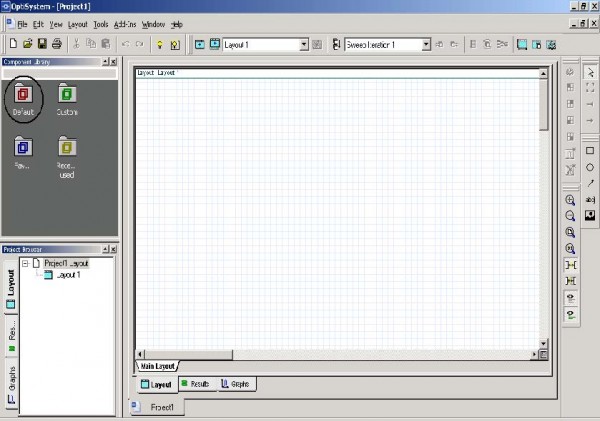
| 2 | To open a new project, from the File menu, select New. The main layout opens (see Figure 12). |
Figure 12: OptiSystem—New project
| 3 | In the Component Library, double-click the Default folder, and then double-click the Optiwave Software Tools folder. The Optiwave Software Tools folder opens and displays the available components. This is where the OptiBPM Component NxM is located. |
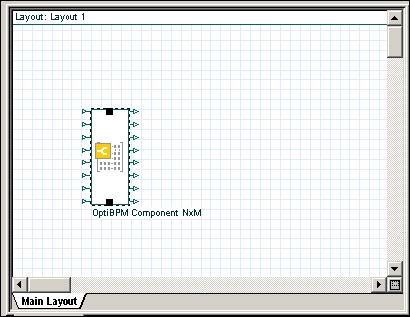
| 4 | Select and drag the OptiBPM Component NxM into the main layout (see Figure 13). |
Figure 13: OptiBPM Component NxM
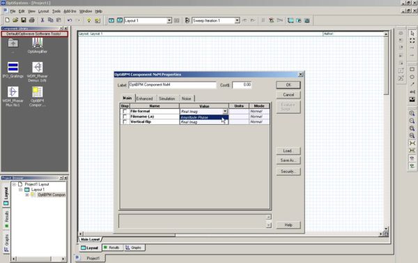
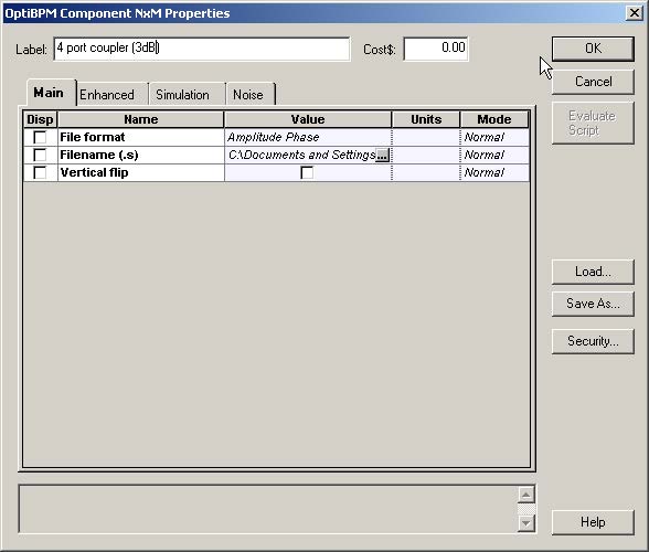
| 5 | To load the scattering data into the OptiBPM Component NxM, in the main layout, double-click OptiBPM Component NxM. The OptiBPM Component NxM Properties dialog box appears (see Figure 14). |
You must select the type of data (Cartesian (Real Imag) or Polar coordinates (Amplitude Phase). The choice must correspond to the data style exported from OptiBPM (Polar in this case).
| 6 | In the OptiBPM Component NxM Properties dialog box, File Format row, select Value > Amplitude Phase. |
Figure 14: OptiBPM Component NxM Properties dialog box
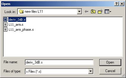
| 7 | To open the s_data.s file, under Value, click The Open dialog box appears (see Figure 15). |
Figure 15: Open dialog box
| 8 | Select the deriv_3dB.s file and click Open. The deriv_3dB.s file path appears under Value. |
| 9 | In Label, describe the device according to the simulation in OptiBPM (in this case we use “4 port coupler (3dB)”) (see Figure 16). |
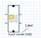
| 10 | Click OK. The OptiBPM Component NxM becomes a 2×2 element—two inputs and two outputs (see Figure 17) and the label changes. |
Figure 16: Final step of loading *.s file
Figure 17: Loaded 2×2 OptiBPM Component NxM—4 port coupler (3dB)
Loading the files for both Arms
To load the arm files, perform the following procedure.
Note: There are options available in OptiSystem that save time when loading/copying files into layouts. Moreover, Optisystem keeps recently used files under the identically called folder. You can simply open the folder and drag the OptiBPM component, if recently used.
| Step | Action |
| 1 | Select the 4 port coupler (3dB) in the layout and right-click. A context menu appears. |
| 2 | Select Copy, place the cursor in the layout, right-click and select Paste. A copy of the 4 port coupler (3dB) appears in the layout. or |
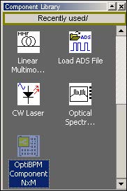
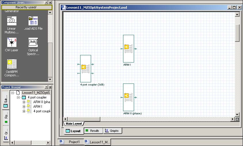
| 3 | Select the Recently Used icon in the Component Library browser of OptiSystem. A list of recently used components appears in the Component Library browser (see Figure 18). |
| 4 | Select the OptiBPM Component NxM and drag the component into the layout. An OptiBPM Component NxM appears in the layout. |
| 5 | Load and label Arm I and Arm II (see Figure 20). |
Figure 18: OptiBPM Component NxM in Recently Used list (OptiBPM Component NxM selected)
Having introduced the input coupler and the both arms, the OptiSystem layout should look like Figure 19.
Figure 19: OptiSystem layout after introduction of arms
Completing the layout in OptiSystem
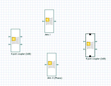
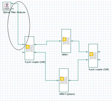
To finish the layout, simply copy and paste the input coupler and move to the right (the *.s file has already been loaded as previously described). Arrange (clicking and moving) the icons to follow the schematics from Figure 1 approximately (see Figure 20).
Figure 20: Components in OptiSystem layout
To add light power to the inputs and detectors of the OptiBPM Component NxM outputs, perform the following procedure.
Note: Because we are studying wavelength response, we will use the Optical Filter Analyzer, which mutually transmits and receives the light from a given interval. The component extracts the frequency response of an optical component by comparing a reference optical signal before and after the calculation.
| Step | Action |
| 1 | To locate the analyzer, double-click on the Default folder, Filters LibraryFilter Analyzer, and select Optical Filter Analyzer. |
| 2 | Disable Autoconnect on Drop in the Layout Operations toolbar. |
| 3 | Select Optical Filter Analyzer, drag the component into the main layout and position it close to the first OptiBPM Component NxM (4 port coupler 3dB) input port . |
| 4 | Double-click on the Optical Filter Analyzer to open the properties dialog box. |
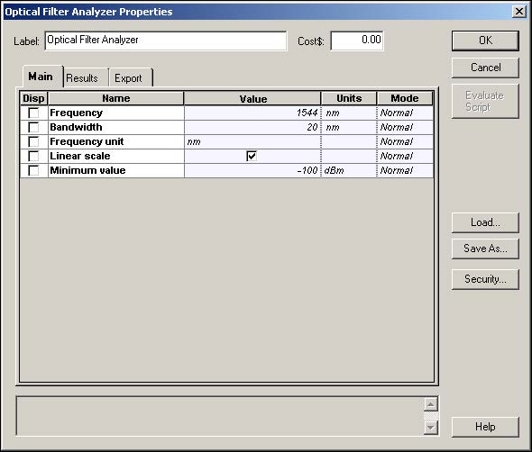
| 5 | In the Frequency unit row, click on Units and select nm (nanometers).
Note: This setting is selected to correspond to the OptiBPM simulation units. |
| 6 | On the Main tab, in the Frequency row, type 1544.
Note: This is the central frequency of the filter analyzer. |
| 7 | In the Bandwidth row, type 20, click on Units, and select nm(nanometers). Note: This is selected to ensure that the filter runs inside the desired interval 1544 nm +/- 10 nm. |
| 8 | Select Linear scale. Note: The results will use a linear scale on the axes. Default is logarithmic (see Figure 21). |
| 9 | Click OK to save the settings and close the dialog box. |
Figure 21: Optical Filter Analyzer Properties dialog box
Connecting the components
| Step | Action |
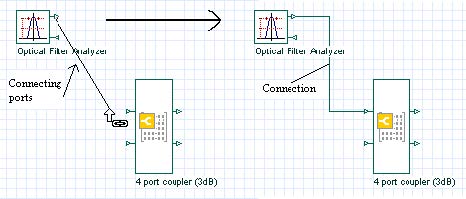
| 1 | To connect the ports, click on the output (upper port) of the Analyzer and connect it to the upper input port of the 4 port coupler(3dB). The components are connected by a green line (see Figure 22). |
Figure 22: Connecting Optical Filter Analyzer to 4 port coupler (3dB)
| 2 | Connect the ports of the arms in the layout as detailed in Figure 23 (follow schematics as shown in Figure 1). |
Figure 23: Inner part of layout connected
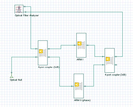
| 3 | Connect the upper output port of the right (output) coupler with the input port of the Optical Filter Analyzer (see Figure 24).
The remaining input port must be assigned to have ‘no’ input field. This is accomplished by using the Optical Null component. |
| 4 | To locate the Optical Null component, in the Component Library browser, double-click on the Default folder, Tools Library, and select Optical Null. |
| 5 | Drag the Optical Null component into the main layout and connect it to the input port of the 4 port coupler (3dB) (see Figure 24). |
Figure 24: The complete layout in OptiSystem environment
Running the calculation
To run the calculation, perform the following procedure.
| Step | Action |
| 1 | From the File menu, select Calculate or Click Calculate |
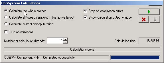
The OptiSystem Calculations dialog box appears (see Figure 25).
Figure 25: OptiSystem Calculations dialog box
| 2 | Click the calculation button After the run is complete, the component internal parameters appear in the layout. Note: To hide the parameters, click the View Port Signal Data (see Figure 26) on the Layout Operations toolbar. |
Figure 26: View Port Signal Data button
Creating the graph to view the results
When the simulation is complete, to create graphs to view the results, perform the following procedure.
| Step | Action |
| 1 | Select the Graphs tab in the layout window. Four empty graph views appear in the layout window. |
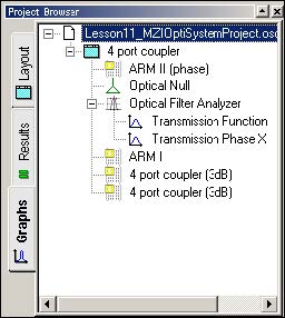
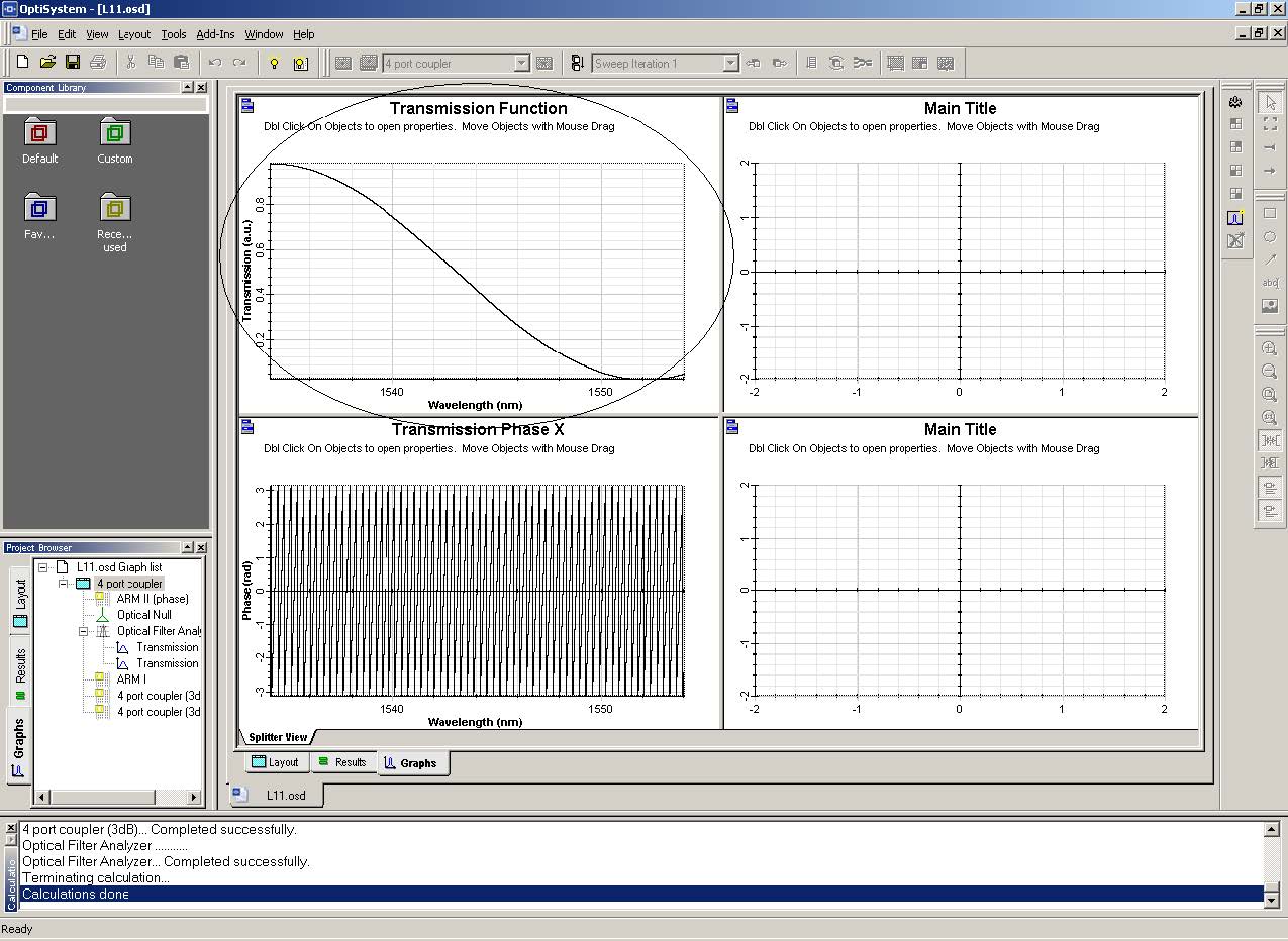
| 2 | In the Project Browser, select the Optical Filter Analyzer icon. Two available graph view titles appear, the power and the optical phase (Transmission Function and Transmission Phase X) (see Figure 27). |
Figure 27: Optical Filter Analyzer under Project Browser
| 3 | Click on the Transmission Function graph icon and move it into one of the graph view quadrants (upper left, for example). The graph appears in the Graph view window (see Figure 28) and the Graph View Type dialog box appears. |
| 4 | Select Current Iteration and click OK.Values for the current iteration are displayed in the graph view.
Note: Once the graphs are defined, any changes made in the layout will automatically appear after the calculation is run. |
Figure 28: Graphs
The power response can be seen in the upper graph. As expected, the power decreases from the maximum (relative units normalized to ‘one’ as for maximum) value to no power at the other end of wavelength spectra.
The lower graph depicts the optical phase as the function of the increasing wavelength within the mentioned interval.
Reference:
[1] Okamoto, K., Fundamentals of Optical Waveguides. Academic Press, San Diego, 2000, Chap. 4.5.


