To define the layout settings, perform the following procedure.
| Step | Action |
| 1 | Type the following settings.
a. Waveguide Properties: Width: 6 Profile: Ti:LiNb03_1 b. Wafer Dimensions: Length: 60 Width: 20 c. 2D Wafer Properties: Material: LN1 d. 3D Wafer Properties Cladding Material: Cladding Thickness: 2 Substrate Material: LN1 Thickness: 10 |
| 2 | To apply the settings to the layout, click OK. |
Designing the waveguide
To design the waveguide, perform the following procedure.
| Step | Action |
| 1 | Draw a linear waveguide in the layout. |
| 2 | To insert the input plane, from the Draw menu, select Input Plane and click at the left side of the layout window.
The input plane appears. |
| 3 | To set up the excitation field properties, edit the input plane properties by selecting Edit > Properties.
The Input Plane properties dialog box appears. |
| 4 | Select the Gaussian. |
| 5 | Click the Input Fields 3D tab. |
| 6 | Click Edit.
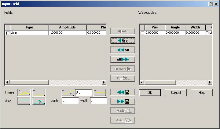
The Input Fields dialog box appears (see Figure 4). |
Figure 4: Input Field dialog box
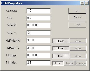
| Since the waveguide is formed by a Ti diffusion, it will be lying just below the top of the substrate. We will therefore set the centre of the beam 3 microns below the surface. | |
| 7 | Click on User |
| 8 | Edit the Field Properties (see Figure 5). |
Figure 5: Field Properties dialog box
| 9 | Close the Input Field and Input Plan dialog boxes to return to the Layout Designer. |


