Now that you have completed Lessons 1, 2, and 3, you are familiar with the basic procedures to create projects using OptiBPM:
- Creating materials
- Inserting waveguides and input planes
- Editing waveguide and input plane properties
- Running a simulation
- Viewing results and various numerical tools in OptiBPM_Analyzer
Lesson 4 and all proceeding lessons provide a high-level description of the procedures you already know. If you require more detailed information, refer to the procedures in the previous lessons.
This lesson describes how to create an MMI star coupler.The MMI star coupler further develops the simple MMI coupler created in Lesson 2: Create a simple MMI coupler. It consists of one input waveguide, an MMI coupler, and four output waveguides. The procedures are:
- Defining materials for the MMI star coupler
- Defining the layout settings
- Creating an MMI star coupler
- Running the simulation
- Viewing the maxima
- Drawing the output waveguide
- Assigning a path to the output waveguide
- Viewing the simulation results in OptiBPM_Analyzer
- Adding output waveguides and viewing the new simulation results
- Viewing the new simulation results in OptiBPM_Analyzer
Before you start this lesson
- Familiarize yourself with the procedures in Lesson 1: Getting Started.
- Familiarize yourself with the procedures in Lesson 2: Create a simple MMI coupler.
- Familiarize yourself with the procedures in Lesson 3: Create a single-bend device.
Defining materials for the MMI star coupler
To define the materials for the MMI coupler, perform the following procedure.
| Step | Action |
| 1 | Create the following dielectric material: Name: guide Refractive index (Re:): 3.3 |
| 2 | Create a second dielectric material: Name: cladding Refractive index (Re:): 3.27 |
| 3 | To save the material, click Store. |
| 4 | Create the following channel: Name: channel 2D Profile definition material: guide |
| 5 | To save the material, click Store. |
Defining the layout settings
To define the layout settings, perform the following procedure.
| Step | Action |
| 1 | Type the following settings. a.Waveguide Properties: Width: 2.8 Profile: channel b.Wafer Dimensions: Length: 1420 Width: 60 c.2D Wafer Properties: Material: cladding |
| 2 | To apply the settings to the layout, click OK. |
Creating an MMI star coupler
Since there are four output channels in the MMI star coupler, it is necessary to find where the simple MMI coupler in Lesson 2: Create a simple MMI coupler produces four intensity maxima. As seen in Lesson 2: Create a simple MMI coupler, this happens where the second waveguide in the MMI coupler is about 1180-1210μm long.
To create an MMI star coupler and find a pertinent coupler length for the desired coupling, perform the following procedure.
| Step | Action |
| 1 | Draw and edit the first waveguide. a. Start offset: Horizontal: 0 Vertical: 0 b. End Offset: Horizontal: 100 Vertical: 0 |
| 2 | Draw and edit the second waveguide. a. Start Offset: Horizontal: 100 Vertical: 0 b. End Offset: Horizontal: 1420 Vertical: 0 c. Width: 48 |
| 3 | To apply the settings, click OK. |
Inserting the input plane
To insert the input plane, perform the following procedure.
| Step | Action |
| 1 | From the Draw menu, select Input Plane. |
| 2 | To insert the input plane, click as close to the left side of the layout window as possible. The input plane appears. |
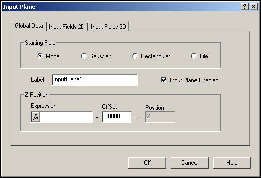
| 3 | To edit the input plane, from the Edit menu, select Properties. The Input Plane Properties dialog box appears (see Figure 1). |
| 4 | Ensure that on the Global Data tab, Z position: Offset, the value is 2.000. |
Figure 1: Input Plane Properties dialog box
| 5 | Save the project. |
Running the simulation
To run the simulation, perform the following procedure.
| Step | Action |
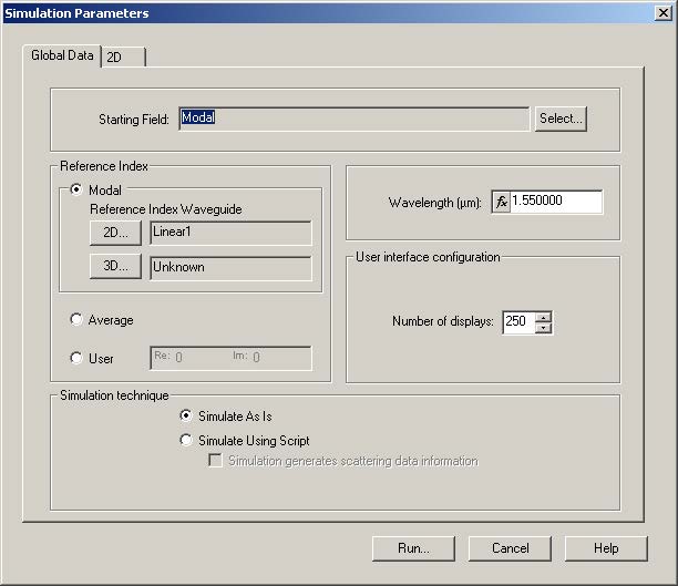
| 1 | From the Simulation menu, select Calculate 2D Isotropic Simulation. The Simulation Parameters dialog box appears. |
| 2 | On the Global Data tab, type 250 in Number of displays. |
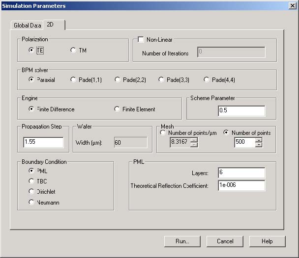
| 3 | Click the 2D tab and ensure that the following settings are selected (see Figure 3). Polarization: TE Mesh – Number of points = 600 BPM solver: Padé(1,1) Engine: Finite Difference Scheme Parameter: 0.5 Propagation Step: 1.55 Boundary Condition: TBC Note: For more information on simulation parameters, see the OptiBPM User’s Guide. |
Figure 2: Simulation parameters dialog box—Global tab
Figure 3: Simulation Parameters dialog box — 2D tab
| 4 | To start the simulation, click Run. The OptiBPM_Simulator window opens and runs the simulation. Note: The simulation in this lesson is short, therefore it will finish quickly. Do open the OptiBPM_Analyzer when you are asked. |
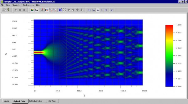
| 5 | Select the 2D Optical Field type view in the OptiBPM_Simulator. Note: To display the 2D view, click the Image Map button |
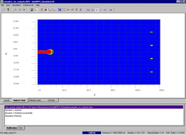
Figure 4: Simulation — 2D Optical Field
Here we can review the results and decide where the coupling will be most efficient and reasonable. As previously discussed, we are interested in the four local intensity maxima and finding their precise horizontal positions.
Since we have 200 displays and the total length is 1420μm, we recognize that these maxima lay approximately within the interval 1400μm from the origin.
Viewing the maxima
To view the maxima, perform the following procedure.
| Step | Action |
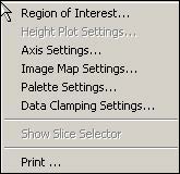
| 1 | In the simulator, right-click in the graph. A context menu appears (see Figure 5). |
Figure 5: Context menu
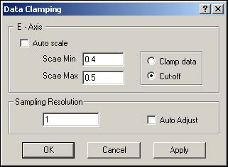
| 2 | Select Data clamping settings. The Data Clamping dialog box appears (see Figure 6). |
Figure 6: Data Clamping dialog box
| 3 | Under E – Axis, clear the Auto scale check box. Scale Min and Scale Max become active. |
| 4 | Type the following values: Scale Min: 0.4 Scale Max: 0.5 Note: The intensity is for the interval <0,1>. |
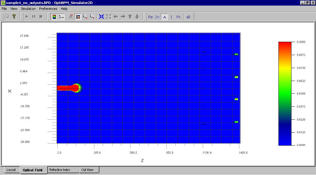
| 5 | To apply the settings to the graph, click OK. The 2D Optical Field view changes to display the new data clamping settings (see Figure 7). |
Figure 7: Simulation with new data clamping settings
| 6 | To view these four points more accurately, right-click anywhere in the graph to access the context menu. |
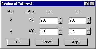
| 7 | Select Region of interest. The Region of Interest dialog box appears (see Figure 8). |
Figure 8: Region of Interest dialog box
| 8 | Type the following values: Axis Z Start: 0 End: 100 Axis X Start: 0 End: 599 Note: The settings you type for the region of interest recalculate the length and width of the graph in points instead of in μm. Therefore, the length changes from 1420μm to 251 points, and the width changes from 60μm to 600 points. |
| 9 | To apply settings, click OK. The view of the simulation zooms into the region that you selected (see Figure 9). Note: Repeat this procedure until the view is satisfactory. |
Figure 9: Simulation — Region of interest
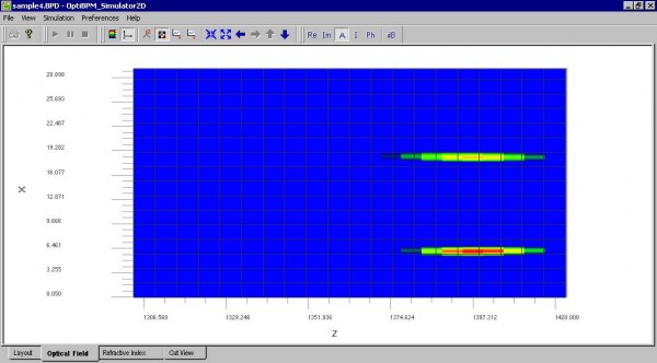
This view shows that the centers of the two points are at approximately 1399μm on the axis.
Note: A procedure that describes this value more precisely is shown in a later lesson that discusses scripting.
| 10 | Close the simulation window and return to OptiBPM_Designer. |
| 11 | To focus more precisely on the centers of the points, change the length of the second waveguide. a. Double-click on the waveguide. The Linear Waveguide Properties dialog box appears.b. Type the following value: End offset Horizontal: 1399 |
| 12 | To apply the setting, click OK. |
| 13 | Change the length of the wafer. a. From the Edit menu, select Wafer Properties. The Wafer properties dialog box appears.b. Type the following value: Length: 1500 (estimated total device length) |
| 14 | To apply the setting, click OK. |
| 15 | Run the simulation (see Figure 10). |
Figure 10: Simulation — Revised waveguide and wafer lengths
Analogically to the procedures above, find a vertical position for the upper and outermost intensity maxima. You will find that it’s approximately 19.6μm.
Drawing the output waveguide
The output waveguide must be on a line that connects the start point of the second waveguide to the intensity maxima.
To draw the output waveguide, perform the following procedure.
| Step | Action |
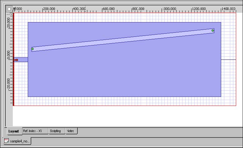
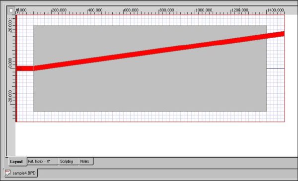
| 1 | Draw the waveguide on top of the second waveguide from 100um to 1500um and at a slight upward angle (see Figure 11). |
Figure 11: Drawing an output waveguide
| 2 | To position the output waveguide accurately, double-click the output waveguide to open the Waveguide Properties dialog box. |
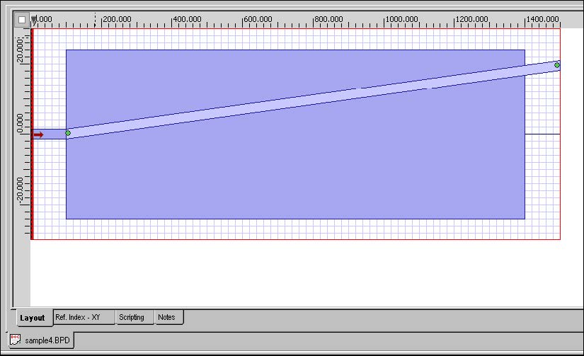
| 3 | Type the following values. Start offset Horizontal: 100 Vertical: 0 End offset Horizontal: 1500 Vertical: 19.6 The position of the output waveguide changes according to the setting that you selected (see Figure 12). |
Figure 12: Modified output waveguide
Assigning a path to the output waveguide
To assign a path to the output waveguide, perform the following procedure.
| Step | Action |
| 1 | From the Edit menu, select Edit Mode > Monitor Paths. The Path Monitor dialog box appears (see Figure 13). |
Figure 13: Path Monitor dialog box
| 2 | Click New. The buttons in the dialog box change (see Figure 14) and the cursor changes into a link. |
Figure 14: Path Monitor dialog box — different buttons
| 3 | In the layout window, click the first waveguide and the output waveguide. The defined path turns red (see Figure 15). |
Figure 15: Red waveguides
| 4 | To apply the path, click Finish. Path1 appears in the drop-down list (see Figure 16) |
Figure 16: Creating Path1
| 5 | To return to the layout window, click OK. The first waveguide and output waveguide change back to the original color in the layout window. |
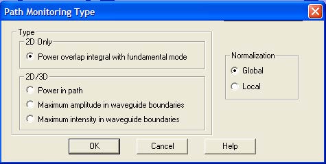
| 6 | In the Layout Window, go to Simulation >> Path Monitor Type… and Select Power overlap integral with fundamental mode with Global Normalization. |
Figure 17: Path Monitoring Type
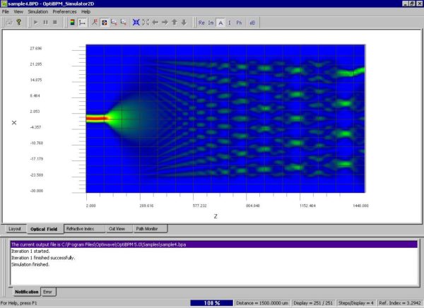
| 7 | Run the simulation and view the output waveguide in the simulator (see Figure 18). |
Figure 18: Simulation with output waveguide
Viewing the simulation results in OptiBPM_Analyzer
To view the simulation results in OptiBPM_Analyzer, perform the following procedure.
| Step | Action |
| 1 | In the dialog box that appears after the simulation ends, click Yes. OptiBPM_Analyzer opens. |
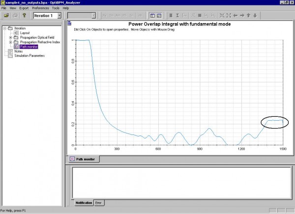
| 2 | In the OptiBPM_Analyzer, select Iteration > Path Monitor. The Path Monitor view appears (see Figure 19). |
Figure 19: Simulation results — Path Monitor view (one path)
The goal is to maximize the coupling from the intensity maxima to the output waveguide. The highlighted section of the graph must be at its maximum level. This is done by precisely changing the vertical end point of the output waveguide. After this iteration, you may find that the coupling is best when the vertical end point value is 19.86μm.
| 3 | To return to the layout window, close OptiBPM_Analyzer, and then close OptiBPM_Simulator. |
| 4 | In the Waveguide Properties dialog box, change the end offset value of the output waveguide to 19.86μm. |
Adding output waveguides and viewing the new simulation results
To add output waveguides and view the new simulation results, perform the following procedure.
| Step | Action |
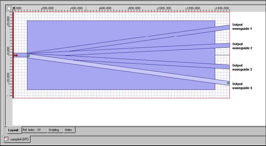
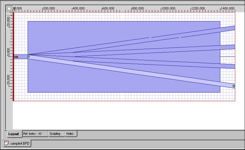
| 1 | Draw three additional output waveguides (see Figure 20).
Note: Since the maxima are distributed symmetrically, a simple trigonometric calculation provides the settings to use for the additional output waveguides. |
Figure 20: Additional output waveguides
| 2 | Position the additional output waveguides as follows: a. Type the following values for Output waveguide 2. Start offset Horizontal: 100 Vertical: 0 End offset Horizontal: 1500 Vertical: 6.62 b. Type the following values for Output waveguide 3. c. Type the following values for Output waveguide 4. |
Figure 21: FInal settings for output waveguides
| 3 | To assign paths to waveguides 2, 3, and 4, refer to “Assigning a path to the output waveguide” . |
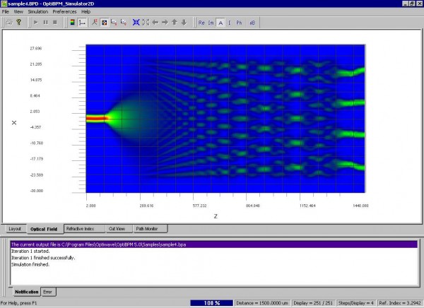
| 4 | Run the simulation (see Figure 22). |
Figure 22: Simulation — four output waveguides
Viewing the new simulation results in OptiBPM_Analyzer
To view the simulation results in OptiBPM_Analyzer, perform the following procedure.
| Step | Action |
| 1 | To open OptiBPM_Analyzer, in the prompt box that appears after the simulation ends, click Yes. OptiBPM_Analyzer opens. |
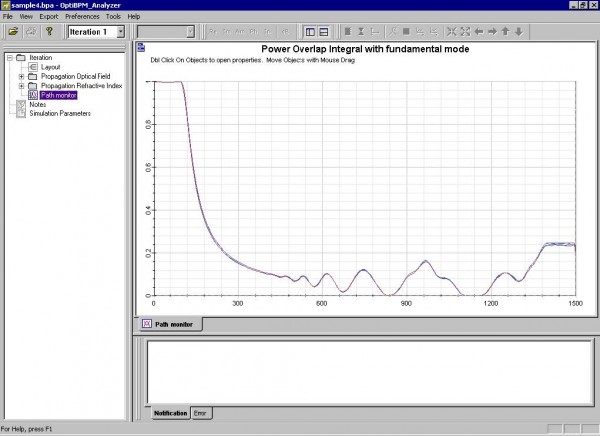
| 2 | In the OptiBPM_Analyzer directory, select Iteration > Path Monitor. The Path Monitor view appears (see Figure 23). |
Figure 23: Simulation results — Path Monitor view (four paths)
As you can see, the resulting paths are very similar. This means that the power distribution in all four output waveguides is almost identical, which reflects the desired result.


