
To define the layout settings, perform the following procedure.
| Step | Action |
| 1 | Click the Default Waveguide tab. |
| 2 | Type the following value:
Width: 4.0 Note: All waveguides will use this setting as the default thickness. |
| 3 | In the Profile list, click ChannelPro1 (see Figure 12).
Note: Both the default setting and the association of any individual waveguide can be changed at any time (in the Waveguide Layout Designer, select Edit > Default Waveguide). |
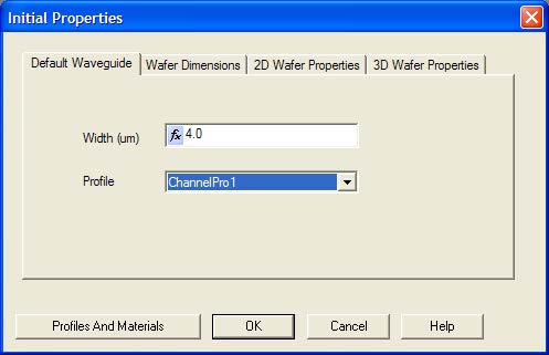
Figure 12: Initial Properties dialog box—Default Waveguide tab
| To specify the size of the region of analysis in the planar view: | |
| 4 | Click the Wafer Dimensions tab.
Type the following values (see Figure 13). Length: 800 Width: 40 |
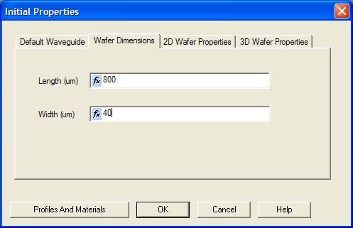
Figure 13: Initial Properties dialog box—Wafer Dimensions tab
| To specify what material to associate with any point that is not contained inside a waveguide (for 2D calculations): | |
| 5 | Click the 2D Wafer Properties tab. |
| 6 | In the Material list, click Silica Cladding.
In the case of 3D calculations, more information needs to be provided, because in general, the material used for the substrate is not the same as the material used for cladding. In addition, the thickness of the layers needs to be specified. In this case, we will define a buried waveguide with the same material in cladding as substrate. Note that this is not the actual thickness of the substrate or the cladding. Instead, these numbers specify the boundary of the calculation window. The ideal thickness for the substrate would be a thickness large enough to contain the guided mode being analyzed, but not so thick that the accuracy of the mesh is compromised. In practice, these dimensions will need to be optimized later, as more experience with the waveguide increases. However, these dimensions can be changed at a later time (in the Waveguide Layout Designer, select Edit > Wafer Properties). To specify the material to be associated with any point not inside any waveguide for 3D calculations: |
| 7 | Click the 3D Wafer Properties tab. |
| 8 | In the Cladding panel, select Material: Silica Cladding, and type Thickness: 17. |
| 9 | In the Substrate panel, select Material: Silica Cladding, and type Thickness: 15. |
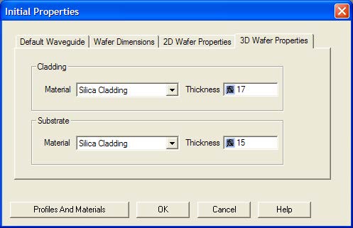
Figure 14: Initial Properties dialog box—3D Wafer Properties tab
| 10 | To apply the settings to the layout, click OK.
The project layout window appears. Note: Maximize the project layout window and adjust the magnification (+ -buttons) so the layout appears as an appropriate size on your screen. |
Save the project as GettingStarted.bpd, so the work done up to this point can be recovered. If you want to keep files that record intermediate steps of this project, use the SaveAs function. After you save the file, the name of the tree in the Profile Designer is “GettingStarted”, the saved name replaces the temporary name “OptiBPMDesigner 1” (see Figure 11). Similarly, if you open other projects in OptiBPM, new tree branches will be created in the Profile Designer with the same name as the newly created project.
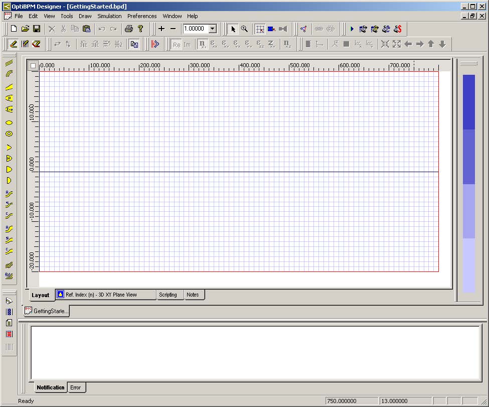
Figure 15: Layout window