Overview
The large negative electric permittivities of noble metals permit the design of sub-wavelength optical guiding structures. In particular, the negative permittivity allows guided modes to exist at single interfaces between the metal and a positive dielectric. These Surface Plasmon Polaritons (SPPs) have extreme electric intensities near the metal-dielectric interface and are commonly used in sensing applications, since they are sensitive to any changes near the interface. Using a 2D mode solver the guided modes of 3D structures can be found.

Applications
- – Sub-wavelength optics
- – Sensing
- – Signal transmission
- – Optical polarizers
- – Bent waveguides
Benefits
- – High aspect ratio waveguides offer no challenge to VFEM mode solver
- – Search for modes with a modal index that is complex
- – Higher order interpolatory hybrid vector/nodal elements, can accurately capture the high electric field intensities near the metal-dielectric interface
- – Triangular mesh size can be adapted to the material properties for higher accuracy
- – Exploiting the symmetry of the waveguide, the simulation domain can be reduced and modes with certain symmetries can be targeted
- – VFEM is very fast and accurate
Simulation Description
The vector finite element method (VFEM) mode solver accepts materials with complex electric permittivities and is formulated with vector basis functions that are particularly well suited for modelling high contrast dielectric interfaces. A good example of this ability is when the VFEM mode solver is applied to plasmon polariton guiding structures.
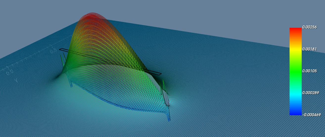
The structure under study is shown on the reverse side as the black contour line, and consists of a core region of silver surrounded by a dielectric with permittivity 4. The silver material has a permittivity of –19 – j0.53 at a wavelength of 633 nm [1]. This guiding structure does not only consist of a high permittivity contrast, but also has a high aspect ratio as it is much wider than it is thick.
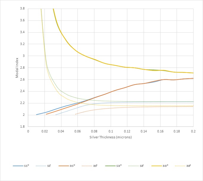
Using combinations of symmetric boundaries and classifying the modes as in [1], a dispersion plot of the modes with respect to the waveguide thickness is shown in Figure 1. All of the modes have a major Ey component, which is consistent with the TM modes found for an infinitely wide structure.

Figure 1: Modal index as a function of silver thickness
For small values of the thickness some of the modes exhibit low loss, for example the ss0 mode, where the Ey component is symmetric about x and y axes. The ss0 mode is of considerable interest, because in addition to its low loss, its Poynting vector is similar in shape to the fundamental mode of an optical fiber (HE11) [1].
The Poynting vector of the ss0 mode along the axis of propagation is shown on the reverse side; Notice how the power is confined to the interface more than to the core. The small part of the Poynting vector that is inside the core is negative, meaning power is flowing against the direction of propagation.
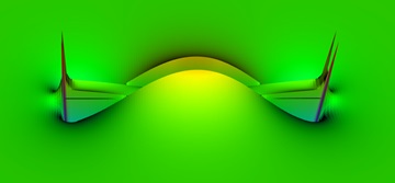
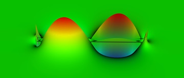
The real part of the Ey field is plotted in the figures below for some different modes of this waveguide. The modes are classified according to the symmetry of the Ey field about the y and x axes, “s” and “a” for symmetric or asymmetric. A superscript is added that describes the number of extrema along the x axis [1].

Figure 2: ss1 mode Re(Ey)

Figure 3: aa2 mode Re(Ey)
The triangular mesh, not shown, is adapted to the large absolute value of the silver region’s permittivity and accurately approximates the field at the corner regions. The rectangular grid used to display this mode is the reason the corner regions appear rough. This is another advantage of a nonuniform triangular mesh.
References
[1] P. Berini, “Plasmon-polariton waves guided by thin lossy metal films of finite width: Bound modes of symmetric structures,” Phys. Rev. B, vol. 61, no. 15, pp. 10484–10503, Apr. 2000.

