This lesson illustrates how to simulate a simple dispersion compensated link elaborating further the concepts of subsystem definition.
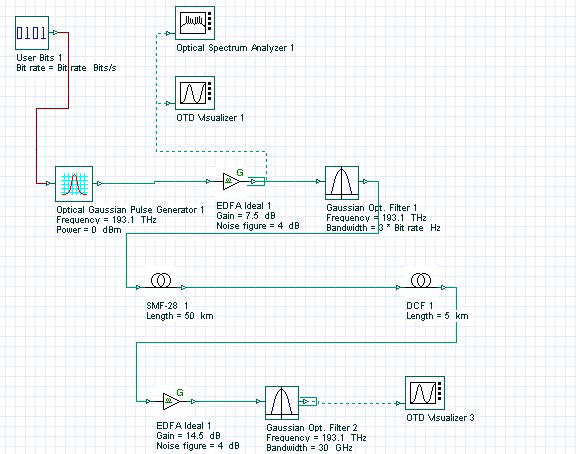
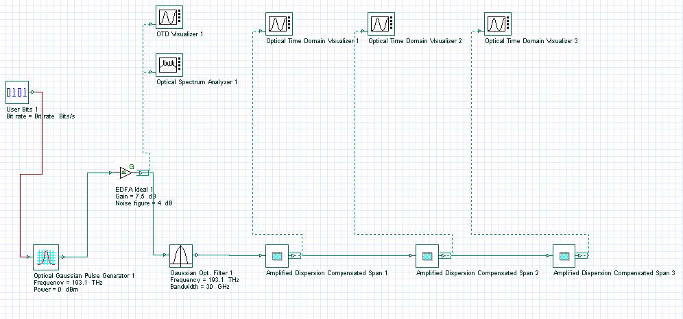
Let us set up the following layout, which includes:
Figure 1: Dispersion compensated link span
- An abstract source of Gaussian RZ pulses according to a user defined bit sequence
- Booster amplifier and filter
- SMF and DCF
- Inline amplifier and filter
- Visualizers
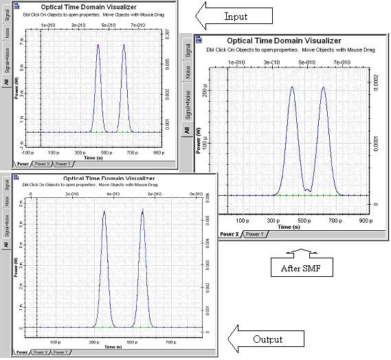
Let us examine the signal waveforms at the input, after the SMF and at the end of the span. One can observe that after the SMF the signal pulses are attenuated, broadened by a factor of approximately 2 and that there is considerable inter-symbol interference.
Figure 2: Signal evolution in a dispersion compensated link span
We can now use the powerful scripting feature of OptiSystem in order to avoid the necessity to redefine those of the layout parameters that depend on the signal in case input signals change. One such parameter is the bandwidth of the two inline filters. Open the filter parameter dialog box and switch the Mode of the Bandwidth to Script. Right-click In the value field and select Bit rate. Then add 3 * so that the whole field reads 3 * Bit rate.
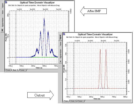
Click on the layout work space and show the Global parameters dialog box. Increase the bit rate twice and recalculate. The following figure shows that regardless of the severe dispersive broadening in the SMF, the signal is again preserved after the whole span, both in terms of power and pulse shape.
Figure 3: Results of the scripted calculations of a dispersion compensated link span Chances
Chances are that this single link might be useful for building longer multi-span systems. In that case it is recommended to encapsulate it into a sub-system, which would later on allow reproducing the same combination of components quickly and efficiently.
We create a new design version, selecting Design Version/ Add Design Version from the main menu of OptiSystem and change its name to Amplified Dispersion Compensating Subsystem. After that we copy and paste all the components of Version 1 in it.
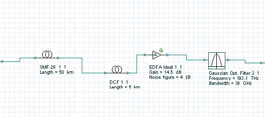
Next, as shown in Lesson 2: Subsystems – Hierarchical simulation, we select all the components, except the signal source and the booster amplifier (including or skipping the visualizers), and select Create subsystem from the right click context menu. Our layout collapses into the visual representation of a subsystem. First we create an output port in the subsystem by selecting Look Inside from the right-click menu and using the Output port tool. After that we can change the name of the new subsystem to something informative, for instance Amplified Dispersion Compensated Span, using the Component Parameters menu item.
Figure 4: The dispersion compensated span represented as a subsystem
Next we can use the newly created subsystem to build longer multi-span links. Let us create another design version and change its name to “Multi-Span Link”. After that, we copy and paste all the components of “Amplified Dispersion Compensating Subsystem” in it.
Now we can arrange a three span system by copying and pasting the “Amplified Dispersion Compensated Span” subsystem component and linking the respective input and output ports.
Figure 5: Building multi-span system using the user defined subsystem
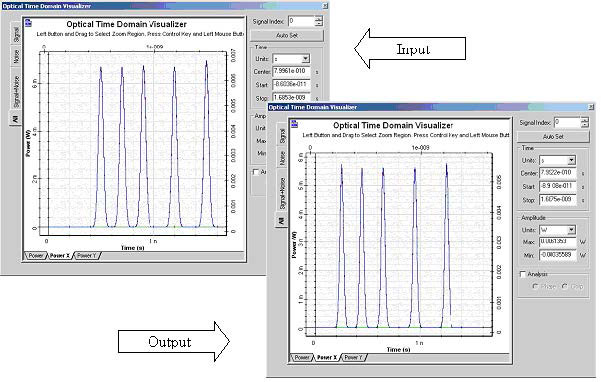
Let us now define a more complex waveform and perform the calculation. After that we can display and compare the input and output signals in terms of their amplitude and pulse shape.
Figure 6: Input and output waveforms of the dispersion compensated links


