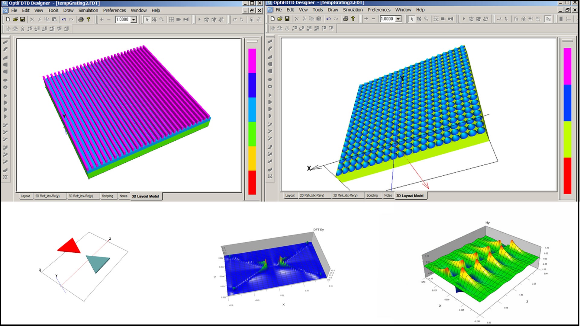
FDTD Benefits
• Presents global overview of photonics problems
• Provides broad material choice
• Offers extensive excitation selection
• Delivers powerful Post-Data Processing
Applications for FDTD
• Photonic band gap materials and devices
• Optical micro-ring filters and resonator
• Grating-based waveguide structures
• Diffractive micro-optics elements
• Complex integrated optics structures
• Nonlinear materials,dispersive materials,surface plasma and anisotropic materials
• Photonic surface plasmon and surface plasma wave
• Nano-partical, cells, tissue and lens
• Electromagnetic phenomena
Next Generation FDTD Simulation Engine
With the 64-bit features of Optiwave’s FDTD, users can design and run a new generation of 64-bit simulations that address up to four billion times as much memory as 32-bit applications. As engineers tackle larger, more complex real-world problems in their designs, suffcient memory becomes crucial. 64-bit operating systems can utilize 16 TB (Terabytes) of RAM. A 32-bit system can only handle a maximum of 4 GB of RAM, severely limiting the amount of accessible memory in an existing system.
Total Field Scattering Field (TF/SF)
Arbitrary tilting plane wave excitation algorithm that separates total field and scattering field. Ideal for Radar Cross Section (RCS) analysis and grating simulations.
FDTD Heating Absorption Module
Metallic and lossy materials in semiconductor devices or solar cells absorb part of the wave energy and convert it to heat. The advanced heating absorption module in Optiwave’s FDTD supports calculations of the heating field distribution and heating absorption rate estimation.
Initial Phase of the Plane Input Wave
Enables users to select the initial phase offset of a launched input wave. A practical application when analyzing combined signals from multiple input planes.
FDTD – Most extensive material choices, including:
• Lossless and lossy materials
• Isotropic and anisotropic materials
• Multiple resonance dispersive materials
• Lorentz-Drude materials – Noble metals and surface plasma materials
• 2nd-Order and 3rd-Order nonlinear materials
• Kerr effect materials
• Raman effect materials
• Perfect conductor materials
FDTD – Most extensive selection of excitation sources, including:
• Waveguide mode excitation
• Gaussian beam excitation
• Plane wave excitation
• Point source and Dipole Source
• Single wavelength excitation
• TF/SF excitation
• Spectral excitation
• Power and amplitude
• Linear or circular polarization
• Multiple beam excitations
Advanced Boundary Condition in FDTD
Optiwave’s FDTD includes an advanced boundary condition simulation feature which optimizes memory usage and provides more accurate results. Using the Uniaxial Perfectly Matched Layer (UPML) method to calculate the absorbing boundary condition in comparison with conventional PML. The periodic boundary condition, Perfect Electric Conductor (PEC) and Perfect Magnetic Conductor (PMC) boundary conditions can be used with UPML to realize more advanced simulations for periodic and symmetric layouts.
FDTD’s Robust Photonic Crystal Editor
Included with Optiwave’s FDTD is a robust photonic crystal editor allowing users to edit any lattice structure and periodic layout with a number of template shapes (i.e. Atom Waveguides). Editing features have also been improved, including user-defned shape creation and structure rotation.
Simulation Automation through Scripting
A powerful feature empowers users with full simulation engine automation through Visual Basic scripting. Completely integrated with the graphical user interface, the fexible scripting tools allow for a streamlined automation process:
• Quickly and easily convert any layout design or its parts into the script.
• Create custom libraries of scripts that represent particular components, which can be added to any new layout design.
• Easily create the most complex design without manual graphical user interface operations.
• Optimize your simulation with comprehensive postprocessing tools.
FDTD Band Solver
A fully integrated 2D band solver is based on the FDTD method with Bloch’s periodic boundary condition, and can generate the band diagram based on the reduced simulation domain of single or multiple cells from a square or hexagonal lattice.
FDTD Waveguide Tapering Options
Waveguides can now be tapered in thickness in addition to width. Channel waveguides can be tapered linearly, and fbers can be tapered linearly and proportionately. With 3D fber profles, the width of the 2D waveguide in the x-z plane is also applied to the height, in order to model fber tapering. As the dimensions change in y, the position of the center line of the fiber in 3D space is mainained.
Post Data Analysis
Optiwave’s FDTD has the strongest post-data analysis tools available. Options include, Discrete Fourier Transform Field Distribution in Domain, Poynting Vector in Domain, Polarized Power calculation, and Overlap Integral calculation.
FDTD Lorentz-Drude model
A Lorentz-Drude model for metallic integrated photonic circuits. This advanced materials model will allow users to perform more accurate, truly full-wave simulations for metallic structures – another “industry frst” captured by FDTD.
FDTD PWE Band Solver
A new band solver based on plane wave expansion (PWE) method will enable customers to analyze properties of photonic crystal materials and devices in all three dimensions.


