This lesson outlines the design process of an electro-optic 2×2 switch based on integrated Mach-Zehnder interferometer.
An electro-optic switch is a device used in integrated fibre optics. The device is based on Mach-Zehnder interferometer made by Titanium diffusion in Lithium Niobate substrate. The switching between the ports is achieved by an electro-optic effect within such structure. Voltage, applied to the electrodes deposited on the integrated Mach-Zehnder interferometer, creates an electric field distribution within the substrate, which consequently changes its refractive index. If properly designed, the induced change in the refractive index leads to different coupling between individual ports.
Design steps
- CAD design of the circuit layout
- Definition of an electrode region
- Definition of an input field and simulation run
Before you start this lesson
- Familiarize yourself with the procedures in Lesson 1: Getting Started.
The procedures are:
- Defining the materials
- Creating the Ti-diffused profile
- Defining the Wafer
- Creating the device
- Defining the electrode region
- Defining the input plane and simulation parameters
- Running the simulation
- Creating a script
CAD design of the circuit
We assume that the integrated switch is created on a z-cut wafer of Lithium Niobate and is surrounded by air cladding. The device is oriented along the Y-optical axis of the Lithium Niobate. Therefore, we need to define a diffused material for the substrate and a dielectric material for cladding.
Defining the materials
| Step | Action |
| 1 | Open a new project in the Layout Designer. The Initial Properties dialog box appears. |
| 2 | Click Profiles and Materials. The Profile Designer opens. |
| 3 | In the Profile Designer, create the following diffused material: Crystal name: Lithium_Niobate Crystal cut: Z Propagation direction: y |
| 4 | Create the following dielectric material: Name: air Refractive index (Re): 1.0 |
Creating the Ti-diffused profile
The waveguides of Mach-Zehnder interferometer are created by diffusion of Titanium in Lithium Niobate substrate. We will need only one Ti-diffused profile :
| Step | Action |
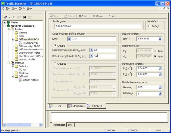
| 1 | In the Profile Designer, create the following Profile: Profile name: TiLiNbO3 Pro1 |
| 2 | Select the Group I panel For Lateral Diffusion length , enter 3.5 For Diffusion Lenght in depth , enter 4.2 |
| 3 | Close the Profile Designer The Layout Design appears. |
Figure 1: Ti:LiNb03 Pro1 Profile
Defining the Wafer
The whole switch device will be about 33 mm long and will not be more than 100 microns wide.
Define the following parameters for the wafer in the Layout Designer:
| Step | Action |
| 1 | In the Initial Properties dialog box, Waveguide Properties tab, type/select the following: Width []: 8.0 Profile: TiLiNbO3 Pro1 |
| 2 | Select the Wafer Dimensions tab and type the following: Wafer Length: 33000 Wafer Width: 100 |
| 3 | Select the 2D Wafer Properties tab and select the following: Wafer Refractive Index—Material: Lithium_Niobate |
| 4 | Select the 3D Wafer Properties tab and type/select the following: Cladding—Material: air Cladding—Thickness: 2 Substrate—Material: Lithium_Niobate Substrate—Thickness: 10 |
| 5 | Click OK to save the settings. |
Creating the device
Tip: to view the whole substrate, it can be useful to change the setting of the Display ratio (Z/X). To do this, select Preferences > Layout Options > Display ratio, and type 200.
We start by laying down the basic waveguide elements necessary for the construction of the switch.
| Step | Action |
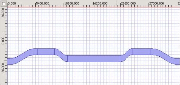
| 1 | In the Layout Designer, create the waveguides listed below (see ): |
| Waveguide name | Start position | End position |
| SBendSin1 | Horizontal: 0 Vertical: -20 |
Horizontal: 5750 Vertical: -7.25 |
| Linear1 | Horizontal: 5750 Vertical: -7.25 |
Horizontal: 9000 Vertical: -7.25 |
| SBendSin2 | Horizontal: 9000 Vertical: -7.25 |
Horizontal: 11500 Vertical: -16 |
| Linear2 | Horizontal: 11500 Vertical: -16 |
Horizontal: 21500 Vertical: -16 |
| SBendSin3 | Horizontal: 21500 Vertical: -16 |
Horizontal: 24000 Vertical: -7.25 |
| Linear3 | Horizontal: 24000 Vertical: -7.25 |
Horizontal: 27250 Vertical: -7.25 |
| SBendSin4 | Horizontal: 27250 Vertical: -7.25 |
Horizontal: 33000 Vertical: -20 |
Note: You can use the mirror and flip operations in Edit > Flip and Mirror menu to build the design.
To build the top waveguides by using the mirror options, perform the following procedure steps for each waveguide in the layout.
| 2 | Select the waveguide on the layout. |
| 3 | Select Edit > Flip and Mirror > Mirror to top. The waveguide is duplicated directly above the selected one. |
| 4 | Double-click on the new waveguide. The properties dialog box appears. |
| 5 | Type the x-coordinates in the horizontal and vertical fields. Note: In order to make the mirror image symmetrical, each vertical coordinate value must be the opposite sign to its counterpart in the original waveguide. |
Example
| Waveguide name | Start position | End position |
| SBendSin1 (bottom waveguide) |
Horizontal: 0 Vertical: -20 |
Horizontal: 5750 Vertical: -7.25 |
| SBendSin5 (top waveguide) |
Horizontal: 30 Vertical: 20 |
Horizontal: 5750 Vertical: 7.25 |
| Linear1 (bottom waveguide) |
Horizontal: 5750 Vertical: -7.25 |
Horizontal: 9000 Vertical: -7.25 |
| Linear4 (top waveguide) |
Horizontal: 5750 Vertical: 7.25 |
Horizontal: 9000 Vertical: 7.25 |
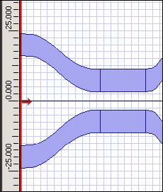
Figure 2: Flip and mirror example
Figure 3: Waveguides created before flip and mirror
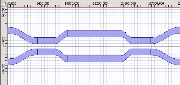
Figure 4: Completed waveguide design
You can check the refractive index profile of different slices through the device.
Checking the RI profile of the x-y slice
To select the z-distance of the x-y slice, perform the following procedure.
| Step | Action |
| 1 | On the Layout Designer, select the Ref. Index (n) – 3D XY Plane View tab located at the bottom of the layout designer window. |
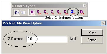
| 2 | On the RI Data toolbar, click the Select Z distance button. The X-Y Ref. Idx View Option dialog box appears (see Figure 5). OR |
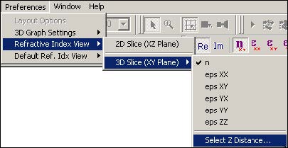
| 3 | Select Preferences > Refractive Index View > 3D Slice (XY Plane) > Select Z Distance (see Figure 6). The X-Y Ref. Idx View Option dialog box appears (see Figure 5). |
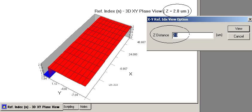
| 4 | In the X-Y Ref. Idx View Option dialog box, type the value for Z Distance and click View. The Ref. Index (n) – 3D XY Plane View is updated to reflect the Z Distance (see Figure 7). |
Figure 5: Z plane selector—RI Data toolbar, X-Y Ref. Idx View Option dialog box
Figure 6: Preferences menu
Figure 7: Refractive Index profile
Defining the electrode region
| Step | Action |
| 1 | Click the Layout tab. |
| 2 | Click the Electrode Region tool.
|
| 3 | Click on the layout where you want to place the beginning of the region and move the mouse to the point where the region should end. The electrode region appears in the layout. |
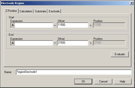
| 4 | Double-click on the electrode region. The Electrode Region dialog box appears (see Figure 8). |
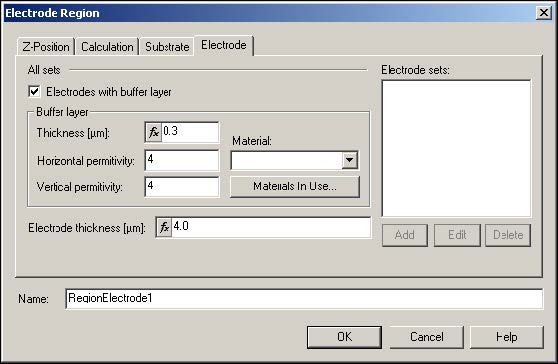
In the Electrode Region dialog box, you can edit the start and end position of the region (Z Position tab), change the reference refractive index and propagation step in the region (Calculation tab), change material properties of the cladding, substrate, and substrate layers (Substrate tab). The Electrode tab allows you to define the electrodes on the substrate. The electrode region in this lesson starts at 11500μm and ends at 21500μm.
Figure 8: Electrode Region dialog box
In this example, we want to build electrodes on the top of a buffer layer. The properties of the buffer layer can be defined under the Electrode tab (see Figure 9). As we did not define a buffer material when we began the lesson, we have to do so now.
Figure 9: Electrode tab
To define the buffer material, perform the following procedure.
| Step | Action |
| 1 | On the Electrode tab, select All sets > Electrode with buffer layer. The Buffer Layer panel is activated. |
| 2 | Click Materials in Use. The Profile Designer appears. |
| 3 | Create a new dielectric material. |
| 4 | Type/select the following: Name: buffer Refractive index: 1.47 |
| 5 | Close the Profile Designer. |
| 6 | On the Electrode tab, type/select the following Buffer Layer properties:
Buffer layer
|
| 7 | Under Electrode sets table, click Add. The Electrode Set dialog box appears. |
| 8 | Define the electrode sets as listed below.
Electrode 1 Center Position 5.5 |
| 9 | Click OK to close the Electrode Set dialog box. The electrode data appears in the Electrode set table (see Figure 10). |
| 10 | Click OK to close the Electrode Region dialog box. |
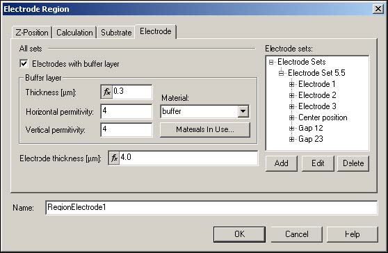
Figure 10: Electrode tab—Electrode set table data
We have specified an electrode region with three electrodes, all with zero voltage, positioned slightly off the symmetry axis of the Mach-Zehnder interferometer.
Defining the input plane and simulation parameters
| Step | Action |
| 1 | Select Draw > Input Plane and place the Input Plane in the layout. |
| 2 | Double-click on the Input Plane on the layout to open the Input Plane properties dialog box. |
| 3 | Type/select the following: Starting field: Mode Z Position— Offset: 0.0 |
| 4 | Click the Input Fields 2D tab. |
| 5 | Click Edit. The Input Fields dialog box appears. |
| 6 | In the Waveguides table, select the second waveguide and click Add. The entry is added to the Fields table. |
| 7 | Click OK to close the Input Fields dialog box. |
| 8 | Click OK to close the Input Plane dialog box. |
To set the simulation parameters, select Simulation > Simulation Parameters, and perform the following procedure.
| Step | Action |
| 1 | In the Simulation Parameters dialog box, Global Data tab, type/select the following: Reference Index: Modal Wavelength μm: 1.3 |
| 2 | Select the 2D tab and type/select the following: Polarization: TM Mesh—Number of points: 500 BPM solver: Paraxial Engine: Finite Difference Scheme Parameter: 0.5 Propagation Step: 1.3 Boundary Condition: TBC |
| 3 | Click OK. |
Running the simulation
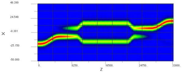
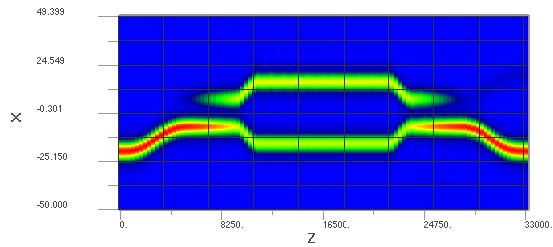
Run the simulation for zero voltage at the central electrode and for 6.75V at the central electrode. You should observe full switching at 6.75V.
To run the simulation, perform the following procedure.
| Step | Action |
| 1 | Select Simulation > Calculate 2D Isotropic Simulation. The Simulation Parameters dialog box appears. |
| 2 | Click Run. The OptiBPM Simulator 2D appears. |
To change the voltage of the central electrode, in the Electrode Region dialog box, Electrode tab, select the electrode set in the Electrode sets table, and click Edit. Type 6.75 in Electrode 2—Voltage (V).
Figure 11: Switching voltage of 0.0V
Figure 12: Switching voltage of 6.75V
You can perform more detailed investigations of the electro-optic switch using scripting language. For example, we can scan the voltage on the central electrode and observe the overlap integral of the output ports with the waveguide mode.
To run the optimization, perform the following procedure.
| Step | Action |
| 1 | Select Simulation > Edit Parameters. The Variables and Functions dialog box appears. |
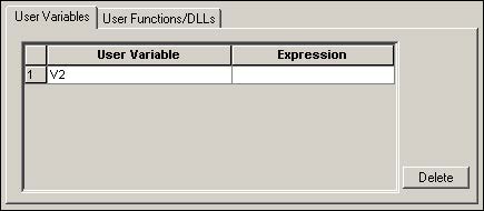
| 2 | To define the variable, type V2 in Name. |
| 3 | Click Verify and click Add. The variable appears in the User Variable table (see Figure 13). |
| 4 | Double-click on the Electrode region in the layout. The Electrode Region dialog box appears. |
| 5 | In the Electrode Region dialog box, Electrode tab, select the electrode set in the Electrode sets table, and click Edit. The Electrode Sets dialog box appears. |
| 6 | Type V2 in Electrode 2—Voltage (V) and click OK to close the Electrode Sets dialog box. |
| 7 | Click OK to close the Electrode Region dialog box. |
Figure 13: User variable V2
| 8 | Select Simulations > Additional Output Data The Additional Output Data dialog box appears. |
| 9 | On the 2D tab, select Power In Output Waveguides, Normalization— Global, and Output Type—Power Overlap With Fundamental Mode. |
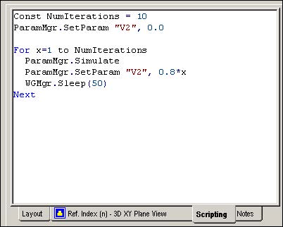
Then we create a simple script, which runs 10 loops increasing voltage V2 from 0.0 to 7.2 V by 0.8V.
Creating a script
To create the script, perform the following procedure.
| Step | Action |
| 1 | Select the Scripting tab at the bottom of the layout window. |
| 2 | Type the following in the scripting window:
Note: You can also first generate a template script by selecting Simulation > Generate Scanning Script and then edit it as shown above. |
| 3 | Before running the simulation, in the Simulation Parameters dialog box, select Simulate Using Script. |
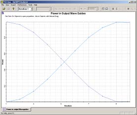
When we run the simple scanning script, we obtain a graph of the optical field overlap versus the number of iterations. It then becomes clear that the electro-optic switch is fully switching the input signal from one output port to another for the second electrode voltage between 6.4 and 7.2V.
Figure 14: Optical field overlap vs iteration


