Base
| Full Name | Jawaduddin Abro |
| Organization | Universiti Malaysia Perlis |
| Job Title | Student |
| Country |
Forum Replies Created
Hi Scott
Sorry, now uploaded .zip file
Thanks
Hi Scott
Sorry, now uploaded .zip file
Thanks
Yeah sorry. Zip file is attached now.
Thanks
Yeah sorry. Zip file is attached now.
Thanks
ohh. Sorry, it failed due to security reasons.
Hi.
Thank you for your reply.
But you can see in my design, Under simulation parameter i cant open the DFT SPECTRUM.
Thats why in my analyzer also Power Spectrum button i cant open.
Do you know the reason?
I wil go through the video also.
Thank you
Hi Scott
I have got my reflectance from observation line 1.
In the above article attached, Structure 1 figure no. 6, they have used refractive index of the external medium as 1.33, 1.36, 1.39.
But i couldn’t find an option where should i have to put an external medium?
Is it in the initial properties under the wafer refractive index?
Please reply as soon as possible.
Your kind response will be appreciated.
Thank you
Hi Scott
thank you for your reply
In observation line 1, i couldn’t find the reflectance, in line 2 with absolute value i find reflectance. Observation line 1 power spectrum graph is not look like reflectance, it is maybe the transmission and reflection is observation line 2 with Absolute value.
Like in the paper above is attached, the structure no 1 results shows graphs reflectance versus wavelength, the graph is dropping at some wavelength which i can see same case in my observation line 2 with absolute value not in the observation line 1.
Please correct me if i am wrong?
Thank you
Hi Scott
Thank you very much for your reply
I am using OptiFDTD v 12.0 Licensed version. My design file (fdt) is attached here.
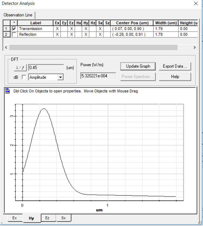
In my design, I have used 2 observation lines, line 1 (reflection) is placed behind the input field for Reflection and line 2 (Transmission) is on the other side to see the transmission. In the simulation parameters under DFT Spectrum, I write 41 as no of samples, and wavelength range from 0.4 to 0.9.
But in the analyzer under Power Spectrum, when i select observation line 1 (Reflection) i can see the graph but i am not sure is it reflection or not?
In observation line 2 (transmission) i got 2 graphs, one is with absolute value and the other is without absolute value. Can you please tell me what is the mean by absolute value? So among all these 3 graphs which i consider for reflection and transmission?
Hope you got my point.
Thank you.
Attachments:
Hi Scott
Thank you for your reply,
Under the observation line, how can i find the reflection spectrum versus wavelength? The observation line file .f2d is attached. This is placed behind the input field.
Thank you.
Hi
thank you for your reply
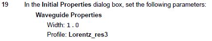
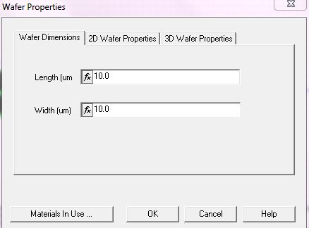
can you explain more where it is in the Edit menu? Its not in the wafer properties. Please see the attachment, this is from the tutorial after we created the profile from the Designer then in the initial properties under the default waveguide tab we need to select its width and the profile (that is missing in Optiwave FDTD v12.0).
Thanks