
Original problem
Photonic Band Gap (PBG) in optical waveguides was first studied at MIT in 1997. The work was published in the ” Letter to Nature”. The Original layout is shown in Figure 1[1]. It is a high contrast ridge waveguide with PBG air holes drilled in the waveguide, the PBG has a defect in the center which will lead to resonance in the wave propagation.
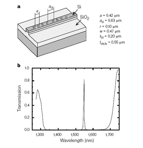
Figure 1: PBG cavity in ridge waveguide and transmission function.
[1] J.S. Foresi, et al. “Photonic bandgap micro-cavity in optical waveguides”, Letter to Nature, VOl. 390, 13, 1997, pp.143.
Project in OptiFDTD
Using the OptiFDTD integrated mode solver, the waveguide mode can be solved and be launched for the FDTD simulation. The time domain beam form is a Gaussian modulated continues wave which covers relatively broad band information.
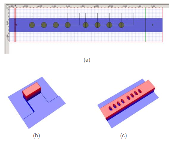
Figure 2: Layout in OptiFDTD
Simulation
For a resonant layout, simulation usually needs more iterations, if we are not sure how many the iterations it should be, we can always select “simulation until user stop” in OptiFDTD. In this case we can check the response in the point detector to determine if the response is convergent or not.
Figure 3 is the time domain response in the point detector and the corresponding normalized spectrum. Blue curve shows the simulation run with 18,000 time iteration steps, while green curve is for 48,000 steps. It can be seen that both curves have the same resonant point, but to get a more accurate Q-value, the simulation needs more iterations.
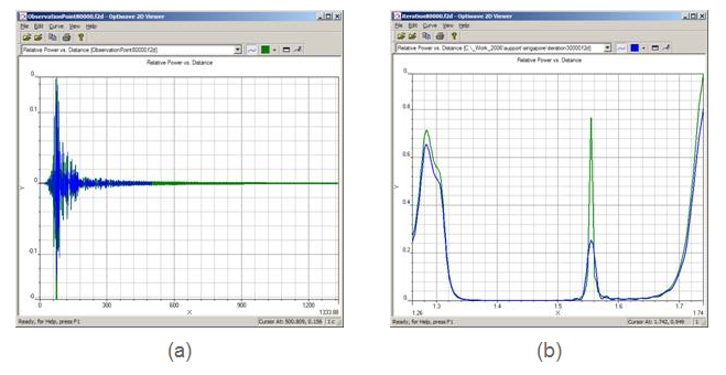
Figure 3: (a) time domain field response in point, (b) normalized spectrum
Transmission function
Please compare the power transmission spectrum in Figure 4 (b) with the published paper in Figure 1, they agree very well. Both the point detector and Area detector can extract the transmission function. However, the point detector will just compare the input amplitude; this requires that the point should be put in the waveguide position where the peak value happens. Area detector will detect the power through the observation plane, so the transmission from Observation area will more accurate than that which comes from the point.
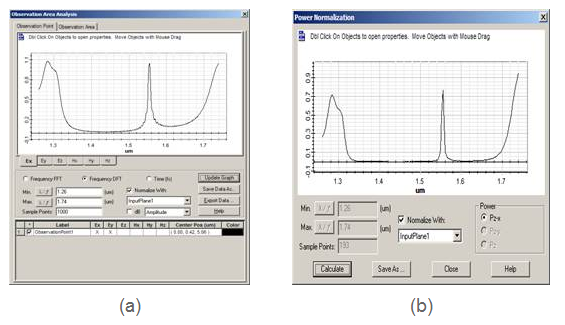
Figure 4: (a) Transmission spectrum from Point, (b) transmission spectrum from Area
Calculate the Quality value (Q-value)
From the power transmission spectrum graph, the resonant wavelength and the bandwidth can be measured in OptiFDTD by using the graph tools, and then the Q-value can be evaluated as shown in figure 5 and the following equation
![]()
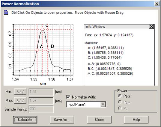
Figure 5: Calculate the Q-value
Observe the guided field mode for different input wavelength.
Observation area will record the field pattern for each sampling wavelength as shown in figure 6.
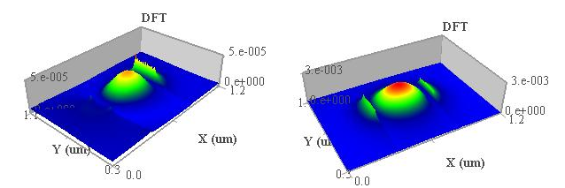
Figure 6: Transmitted field pattern for different wavelengths