What kind of grating layout can OptiFDTD simulate?
Gratings are basically periodic layouts that may contain chirp or apodization. The wave inside the grating may be complex: Scattered field, transmitted field, diffracted field are all exist, which demand more advanced simulation tools for highly accurate results.
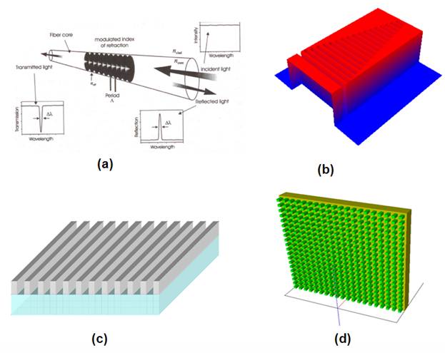
From wave effect, grating layouts can be seen as two groups: Waveguide grating (See Figure 1a and 1b) and surface gratings, or volume gratings (See figure 1c and 1d). OptiFDTD is suitable for all of these grating simulations. The following are samples for Grating simulation and numerical validation.
Figure 1: Selected Grating layout
Metallic surface grating
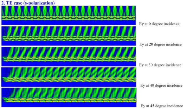
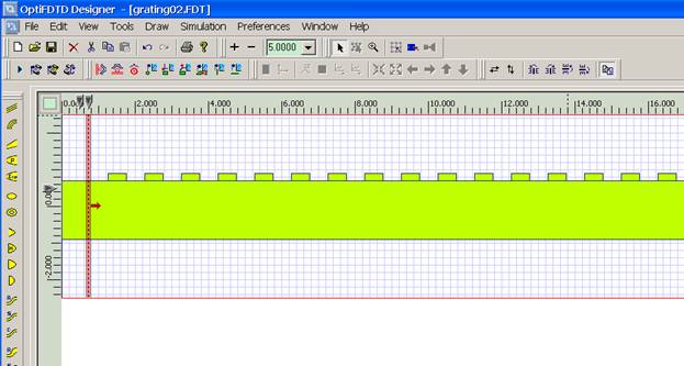
Figure 2 shows a silver surface grating with a plane wave incident at different angles. The layout extends to y-direction for a relative longer distance compared to the input wavelength, so the simulation can be considered as a 2D simulation. The Drude model is used for silver. The periodic silver surface can be designed by VB scripting or the PBG editor.
Figure 2: Silver Grating
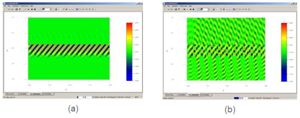
When a tilted plane wave is launched to the layout, the time domain wave propagation can be observed in the simulator. OptiFDTD uses the Total-Field/Scattering field (TF/SF) algorithm for the input wave excitation. This TF/SF technique has the pure reflected wave and transmitted wave in the same simulation[1]. Figure 3(a) is the plane wave response before it accesses the grating surface. Figure 3(b) shows the time domain scattered field, diffraction field and transmitted field.
Figure 3: Time domain field response
After the simulation, a steady state response can be observed in the analyzer. Using VB script the input angle scan simulation can be done.
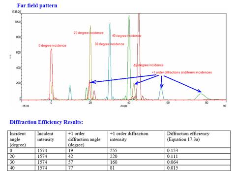
The Slice Viewer in Analyzer allows us to observe the near field in each slice ( see figure 5). Then Far-field transform is used to find the diffraction field direction and diffraction efficiency (see figure 6).
Figure 5: Near field in slice viewer
Figure 6: Far field pattern and Diffraction efficiency
Numerical validation for grating simulation
The first numerical validation for grating simulation is Directional Grating Coupled Radiation in waveguide Structure as shown in Figure 7. The Original layout was published in Reference 2.
Figure 7: Directional grating Coupled waveguide in OptiFDTD
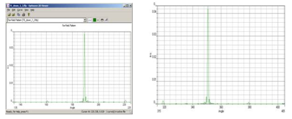
The Diffraction angle is stated as 190.3 and 349.7 in reference [2], OptiFDTD results are shown in figure 8.
Figure 8: Far field in OptiFDTD θ=189.3, 350.7
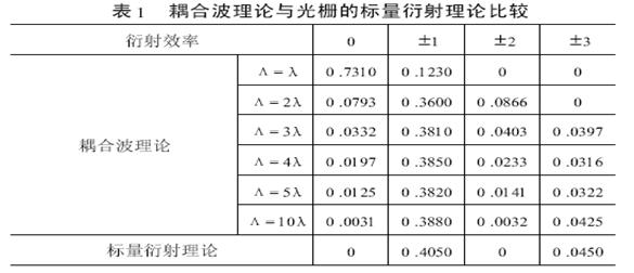
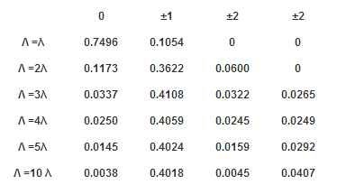
Figure 9: Grating efficiency in reference using couple mode theory (λ is the wavelength and Λ is the pitch length)
Figure 10: Diffraction efficiency Results in OptiFDTD
References
1. Allen Taflove and Suan C. Hagness, “Computational Electrodynamics—The Finite difference Time-Domain Method”, Artech House. 2000
2. in IEEE Journal of quantum electronics, Vol. 40, July2004, Curt,A. Flory, ” Analysis of Directional grating-coupled radiation in waveguide structures”
3. in Laser Journal (in Chinese), VOl. 25, No. 2, 2004, pp.3


