
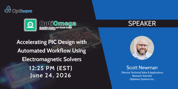
Accelerating PIC Design with
Automated, Multi-Fidelity Workflows
Are you looking to compress your Photonic Integrated Circuit (PIC) design cycles without sacrificing physical accuracy?
In our upcoming online summit, our engineering team will present a comprehensive walkthrough of the automated workflow optimizations powering the next generation of optical design. This session is your fast lane to smarter, faster prototyping.
Here is a quick look at what we will be showcasing:
🚀 What’s New (The Hot Slides):
- Conformal Waveguide Bend Analysis:
Say goodbye to geometric approximations. We are introducing polar-to-Cartesian conformal coordinate mapping W=R2ln(Z/R2)) paired with stretched PML boundary conditions. Now, you can calculate bending losses and effective indices with absolute mathematical rigor.
- Bayesian Multi-Fidelity Optimization:
Why burn GPU hours on raw 3D FDTD sweeps? Learn how our smart Bayesian framework runs rapid 2.5D FEM models to identify high-potential parameters before committing to heavy 3D FDTD simulations.
- DeAP Evolutionary Trajectories:
Optimize complex component geometries automatically using evolutionary algorithms (DeAP) tracked via cumulative explained variance.
🛠️ Robust Foundations (The Solvers You Trust):
- Next-Gen FEM Solver:
Our integrated photonics engine features automatic matching mesh generation, native GDSII import, and rapid 2D/2.5D S-parameter extraction.
- Vector Finite Difference (VFD) Mode Solver:
A workhorse Cartesian grid engine that handles lossy materials, diagonal tensor permittivity, and PEC/PML boundaries seamlessly.
📅 Join the Live Session & Connect with Us!
Don’t design in the dark. Join our technical team live to see these workflows in action, participate in an interactive Q&A, and discuss your specific layout targets.
- Reserve Your Spot for the Live Webinar
- Want a trial license or custom script evaluation? Our team is here to help you bridge the gap from concept to tape-out. Contact us today to discuss your application!