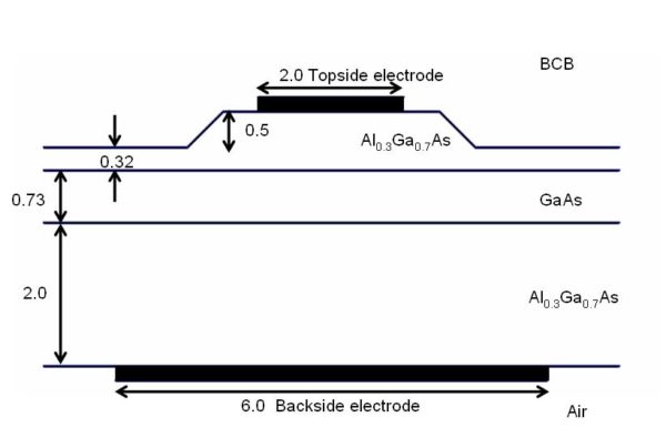
This lesson shows how to make a 3D simulation in a material modified by the linear electro-optic effect (Pockels Effect). The waveguide design of Reference [1] is shown in Figure 1 below. In this lesson, this waveguide is created, a potential is applied to the electrodes, and the results are compared to Reference [1].
Figure 1: This is Fig.2 of Reference 1, drawn upside down. This waveguide is a ‘Substrate-Removed’ design, so the cladding is BCB, a polymer used to glue the waveguide to another substrate, not shown. This mounting exposes the AlGaAs cladding layer to air, and the Backside electrode is evaporated there. All lengths are in microns.
OptiBPM has another, older, electro-optic module. This legacy feature is specialized to three coplanar electrodes when used on diffused electrodes in lithium niobate. See Lesson 14: Mach-Zehnder Interferometer switch. If the system you want to model conforms to this specific case, and information about electrode impedance is not required, you might want to consider the Electrode Region feature described in Lesson 14: Mach-Zehnder Interferometer switch. For all other electro-optic simulations, the feature described in this tutorial should be used.
The material system for this example is AlGaAs. The ridge structure forms a waveguide and supports TE and TM waves, although only the TE mode is excited in our example. The electrodes are metal and do not significantly intersect the guided mode. When the electrodes have a potential difference, a mostly vertical electric field appears in the material that supports the optical mode. The refractive index of the material is modified slightly by the electo-optic effect. The effect is small, but it can make a significant difference in the phase of the optical wave after propagation over a long distance, on the order of one cm. According to Ref [1], applying a potential difference of 17.8 V between the Topside and Backside electrode should cause a change in phase of Pi after 1cm of propagation in the fundamental mode of the waveguide.
To make a project that simulates the voltage-dependent optical phase shift, follow these steps. A finished project can be found in the Tutorial Samples directory, called Lesson10_ElectroOptic.bpd.
It is recommended that you have already finished Lesson 1: Getting Started. It is also a good idea to have already completed Lesson 9: Create a chip-to-fiber butt coupler as well, in order to be familiar with issues in 3D BPM simulation without electro-optic effects.
Define Dielectric Materials
| Step | Action |
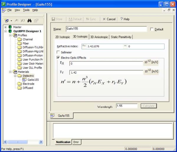
| 1 | In a new project, open the Profile Designer and create a new material for GaAs in the branch Materials/Dielectric. Name the material GaAs155, and enter a refractive index of 3.421076 in the 2D and 3D Isotropic tabs of the new material. This value of refractive index is taken from Reference 2. The electro-optic tensor for GaAs has non-zero components r41 = r52 = r63 in the crystal coordinate system. However, for this device the waveguide axis is rotated in the XZ plane by 45° relative to the crystal axis, so a vertical (parallel to Y) electrostatic field affects the TE mode by an electro-optic coefficient equal to r41. In this project we will simulate a TE mode, so enter the r41 coefficient as rV, the vertical electro-optic coefficient. (select the Electro Optic Effects check box) The horizontal part of the electric field does not affect the horizontally polarized TE mode, so the rH should be set to zero. |
Figure 2: The refractive index and electro-optic coefficients of material GaAs at λ = 1.55 μm. n = 3.421076, rV = 1.42 x 10⁻¹² [m/V]
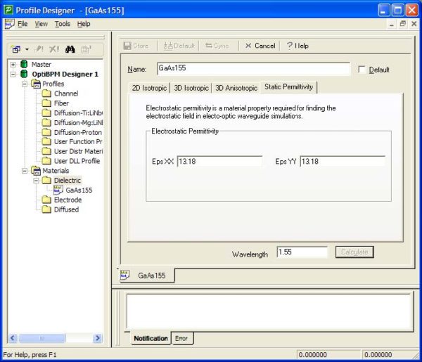
| 2 | Click on the Static Permittivity tab and enter 13.18 for the XX and YY component of the static permittivity tensor[3]. |
Figure 3: Static Permittivity of GaAs.
| 3 | Click on Store to enter the new material into the project. |
| 4 | Repeat steps 1-3 for the other dielectric materials in the project. The names and properties of all dielectric properties in the project are shown in Table 8 below. |
| Name | n | rH| | rV | EpsXX | EpsYY |
| GaAs155 | 3.421076 | 0 | 1.42e-12 | 13.18 | 13.18 |
| A13Ga7As155 | 3.279933 | 0 | 1.42e-12 | 12.244 | 12.244 |
| BCB | 1.538 | 0 | 0 | 2.365444 | 2.365444 |
| air | 1.0 | 0 | 0 | 1.0 | 1.0 |
Table 8: Properties of dielectric materials used in the waveguide of Fig. 1. Refractive index of BCB taken from Ref. 4.
Define Electrode Materials
The definition of a material as an electrode is the way that electrodes are introduced in OptiBPM. Profiles and Waveguides define optical waveguide geometry, and these objects are filled with materials to define the optical refractive index within them. If a material is defined as an electrode material, then the same Profiles and Waveguides used for specifying waveguide geometry can be used for specifying electrode geometry.
In OptiBPM, electrodes are assumed to be perfect conductors. Since there is no electrostatic field inside a perfect conductor, the material properties rH, rV, EpsXX, and EpsYY do not apply to electrodes, and are not found in the electrode material dialog boxes.
The electrodes do have optical properties. This is to permit precise definition of optical properties for devices that have transparent electrodes. In the case of metal electrodes or other electrodes that are not transparent, the electrodes are usually placed far from the optical field of the waveguide, and therefore the optical properties of the electrode are not significant in the device function. In this case, the optical properties of the electrode should not be set to the actual optical properties of metal, but should be set to some value that will not cause numerical trouble with the beam propagation method to be used for simulation. We recommend choosing a real refractive index slightly smaller than the cladding index, or the refractive index of other materials found in the vicinity. In effect, the electrode is made transparent to the beam propagation simulator, and does not participate directly in the optical simulation. The effect of the electrode material is through the electrooptic effect only, as desired in electrooptic devices.
| 5 | In branch Materials/Electrode of the Profile Designer, create a new material called Electrode1 (the default name). Enter 2D and 3D refractive index of 1.6. This material is for a metal electrode, and will be placed far from the optical wave. The refractive index of 1.6 will prevent the electrode from disturbing the beam propagation method of simulation. See comments in the paragraph above. |
| 6 | Click on Store to enter the new material into the project. |
Figure 4: The electrode material Electrode1, n = 1.6
| 7 | Repeat step 5-6 for another material, called ground. Use the same refractive index. |
Define Profiles
| 8 | Create a Channel profile called ridgeWG. This will be placed on top of the epitaxial layers to create the ridge of Figure 1. Set the 2D profile definition to Material Al3Ga7As155. Set the 3D profile definition with one layer of Material Al3Ga7As155 with Width 3, Thickness 0.5, and Offset 0. Enable the Slanted Walls feature, and enter 45° angles on the right and left sides. |
Figure 5: Definition of the ridgeWG Channel Profile
| 9 | Click on Store to enter the new profile into the project. |
| 10 | Repeat Steps 8-9 to create a profile for an electrode. Name the Profile Electrode1Profile and enter the Material as Electrode1 for 2D and 3D profile definitions. Set Width = 1.0, Thickness 0.2, and Offset 0. |
Figure 6: Fig. 6, Definition of Electrode1Profile
| 11 | Repeat Step 10, but name the new profile GroundElectrode. All properties are the same as Electrode1Profile except the electrode material is ground instead of Electrode1 material. |
Figure 7: Definition of Ground Electrode Profile
| 12 | Return to the Initial properties dialog box and enter the following choices: Waveguide Properties tab Width 4.0 Profile: ridgeWGWafer Dimensions tab 12000 Width 40 2D Wafer Properties tab 3D Wafer Properties tab |
| 13 | Click OK |
| 14 | Save the project. |
Draw the waveguide
| 15 | Change the view to see the whole wafer by Preferences >> Layout Options >> Display Ratio = 200. |
| 16 | Select Snap to Grid from the icon in Tools.
Figure 8: Snap to Grid icon |
| 17 | Select a linear waveguide and draw from ( 0, 0) to (12000, 0) |
Figure 9: Layout with ridgeWG profile.
| 18 | With the Select tool, right click in the waveguide to open the Linear Waveguide Properties dialog box, and change the Depth to 3.05 |
Figure 10: Adjust Depth of waveguide Profile to 3.05
| 19 | Open the Simulation Parameters dialog box from Simulation >> Simulation Parameters. In the 3D Isotropic tab, enter Number of Points per micron in X as 10 and 30 for Y. Set the View Cut in X to 201 and to 100 in Y. This box also has a radio button to select which solver will be used to find the electrostatic field. The default is SuperLU, which can be used if your system has sufficient RAM. If there is trouble with this solver later in the project, the solver can be changed to the alternative solver, Bi-Conjugate Gradient. |
Figure 11: Simulation Parameters polarization, mesh, viewcut, and slover settings.
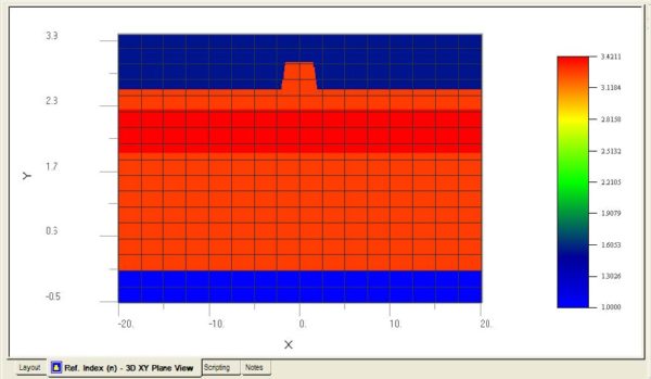
| 20 | Look at the profile so far by clicking on the Ref. Index (n) – 3D XY Plane View tab. The Air substrate, the BCB cladding, and the semiconductor ridge should already be there, as in Figure 12. |
Figure 12: Transverse plane View (XY Plane)
| 21 | The other dielectric layers are input by using the Region feature of OptiBPM. In the Layout select Draw >> Regions >> Substrate Region, and drag and drop the substrate region on the layout. With the Select tool, right click on the new Region to get to the Substrate Region Dialog box. Enter 0 as the starting offset, and 12000 as the end. |
Figure 13: Substrate Region Start and End settings.
| 22 | Go to the Substrate tab and click Add to add the first layer. Enter for the Start and End Thickness 2.0, and select material Al3Ga7As155 |
Figure 14: Substrate Layer
| 23 | Repeat step 22 to add the second layer. Enter for the Start and End Thickness 0.73, and select material GaAs155. |
| 24 | Repeat step 22 to add the third layer. Enter for the Start and End Thickness 0.32, and select material Al3Ga7As155. |
| 25 | Look at the profile again by clicking on the Ref. Index (n) – 3D XY Plane View tab. The substrate layers should be there, to reproduce the waveguide part of Figure 1 |
Figure 15: Waveguide of Fig. 1
Draw the electrodes
| 26 | In the layout view, draw a second linear waveguide with the same coordinates as the first waveguide. With the Select Tool, right click on the waveguide to open the Linear Waveguide Properties dialog box. Change the Width to 2.0, the Depth to 3.55, and the Profile to Electrode1Profile. |
Figure 16: Electrode 1 layout definition
| 27 | The different profiles appear as different shades by default. It might improve the display to right click the graded scale on the right side of the layout and select Properties. The Spectrum type Rainbow will make the profiles different colours. |
Figure 17: Layout Profile Spectrum
| 28 | Repeat Step 26 to draw the ground electrode. Let the Width be 6.0, the Depth be –0.2, and the Profile be GroundElectrode. |
| 29 | This waveguide is wider than the rest, so it covers the first two. Note that right clicking the waveguide presents layout options such as Move To Back. Apply this to this waveguide so that the other two can be seen in the layout. |
Figure 18: Finished layout with Substrate Region, two electrodes, and ridge waveguide.
| 30 | Look at the Ref. Index (n) – 3D XY Plane View tab again. In certain angles of the XY Plane view in the Height Plot mode, one can see the electrodes as well as the waveguide. |
Figure 19: Finished waveguide with electrodes.
Electrostatic Simulation
| 31 | Go to Edit >> Edit Electrodes to get the Edit Electrode Connections dialog box. Each Electrode Material has a combo box with a selection of electrode Ids, there is one ID for each of the Electrode Materials. |
Figure 20: Edit Electrode Connections dialog box, with combo selection of electrode ID.
| 32 | The Electrode ID is used to accommodate the case where two different Electrode Materials are electrically connected outside the layout, and need to be considered as one if electrode capacitance or impedance is to be calculated. In that case, the two Electrode Materials could be assigned the same electrode ID. In this example, there are only two electrodes each with different potential, so assign Electrode1 to Electrode ID 1, and ground to Electrode ID 2. |
| 33 | Once the IDs are assigned, one can assign the potentials in the Electrode Potential list box. Assign a potential of 17.8 V to Electrode ID 1, and 0 V to Electrode ID 2. |
Figure 21: Edit Electrode Connections dialog box, with potentials
| 34 | Close the Edit Electrode Connections dialog box. |
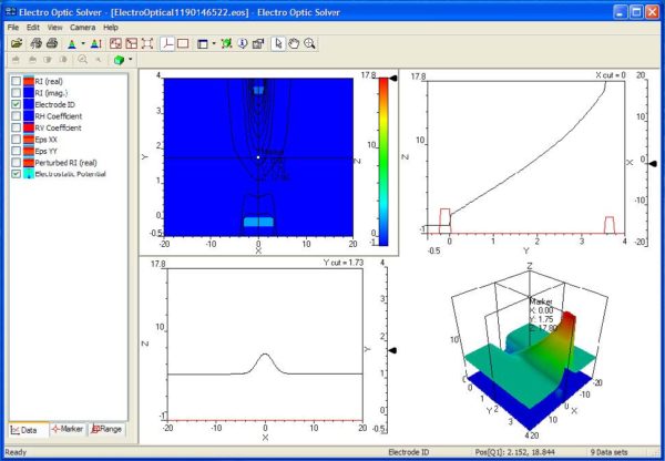
| 35 | Run the Electrostatic simulation by Simulation >> Electro Optical Solver >> Calculate. The Electro Optical Solver window will open, and the graph will initially show the position and ID of the electrodes in this transverse plane. (Position Z = 0 is the default, but this can be adjusted with the slider in the Electro Optical View Option dialog box. ) Selecting Electrostatic Potential in the tree will show equipotential contour lines superimposed on the electrodes. |
Figure 22: Electro Optic Solver. Selecting Electrode ID first and Electrostatic Potential second shows the Electrode ID in colour and the Electrostatic Potential in contour lines. The picture can be more clear by turning off the grid. (Right click and unselect Grid).
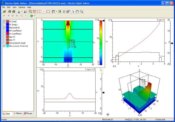
| 36 | Selecting the Electrostatic Potential first, then RI real, and then Electrode ID will show the potential in colour, and the electrode and waveguide boundaries with superimposed lines. |
Figure 23: E Electro Optic Solver.
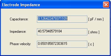
| 37 | Go to View >> Electrode Impedance to see the impedance calculated for these electrodes. This data is available whenever the current Z slice has exactly two electrode IDs with different potential. The Capacitance is from the lumped circuit context, it is the capacitance found between these two electrodes if the length is 1 mm. The impedance and Phase velocity come from the transmission line context. Here it is assumed the two electrodes are part of a balanced transmission line, and that the electrodes are perfect conductors. The calculated wave impedance is given in ohms, and the phase velocity is expressed as a fraction of the speed of light, c. |
Figure 24: Electrode Impedance. Capacitance is for a lumped circuit. Impedance and Phase Velocity are for the balanced transmission line case.
Electro-Optic Simulation
| 38 | In the Layout view, add an Input Plane (see Lesson 1: Getting Started). Set the Z Position to 0 and the Starting Field to Modal. In the Input Field dialog box, select the waveguide with the ridgeWG profile to form the input field. |
Figure 25: Input Field dialog
| 39 | Exit all the input dialogs with the OK button. |
| 40 | Select Simulation >> Additional Output Data >> 3D Isotropic tab, and select Relative Power vs. Distance and Electrode Impedance. In the Z Cut tab, select Field, Refractive index, and Potential and Permittivity for various Z positions. Exit the box with OK. |
| 41 | Start the simulation with Simulation >> Calculate 3D Isotropic Simulation … >> Run… Adjust the simulator view by View >> Optical Field Cut >> XZ Cut, and switch the display from Amplitude to Phase by View >> Complex Data View >> Phase. You will observe a phase shift of over a distance of 1 mm, in agreement with Ref. [1]. |
Figure 26: Simulation of Phase of the guided mode with electrode potential 17.8 V
| 42 | When the simulation finishes, open the Analyser and observe the data in the Electrode Impedance tree. Right click the graph to open the legend. If the electrodes change position over the wafer, this graph will plot the changes vs. Z. Numerical data is available from the Export Data option that drops down from the blue icon at the top left corner of the graph. |
Figure 27: Plot of electrode impedance vs propagation length, Z
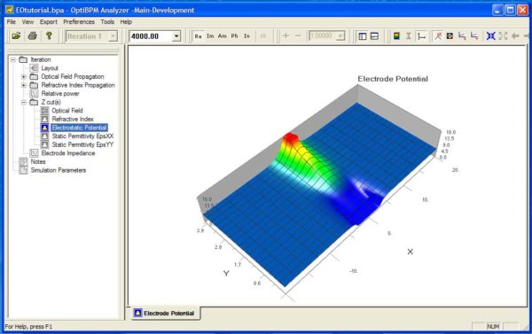
| 43 | Open the Z Cuts directory from the tree and select optical, refractive index, permittivity, or Electrostatic Potential data for display. The Z value is then selected from the combo box. |
Figure 28: Fig. 27, Electrostatic Potential at position Z = 4000.
References
[1]S.R. Sakamoto, A. Jackson, N. Dagli, “Substrate Removed GaAs-AlGaAs Electrooptic modulators”, IEEE Photonics Technology Letters 11(10), p1244 – 1246 (1999)
[2]Adachi and Oe, J. Appl. Phys, 6620 54(11) (1983)
[3]Y. Cui and P. Berini, “Modeling and Design of GaAs Traveling-Wave Electrooptic Modulators Based on the Planar Microstrip Structure”, J. Lightwave Tech., 24(6) p2368-2379 (2006)
[4]Kwon et al., Optics Express Vol. 11 No. 18 p2211- 2215 (2003)


