2.1 Layout design of the diamond lattice
The fcc lattice of air balls in dielectric was not found to posses band gaps. However, it has been shown that in case of diamond lattice band gap structure can be detected. The diamond lattice is composed of two interpenetrating fcc lattices, one displaced ¼ of a lattice constant in each direction from the other. We can easily create such structure in the layout designer by simply adding another fcc lattice.
Save the file under different name to keep the original fcc lattice design. Double click on the fcc layout, the Crystal Lattice Properties dialog box presents. In the “Atom Waveguides in Unit Cell” region, select ‘True 3D Sphere Waveguide” and click new will start to add another atom in the existing fcc layout. Please shift this new atom position by ¼ in all the (x, y, z) direction. Set the two Sphere atom’s radius as 0.325. Check the refractive index and persuade yourself this is indeed a diamond lattice. As reported in [1] the band gap should be maximized for sphere radius of 0.325.
2.2 Set parameters and run simulation
Keep the PWE band solver simulation parameter setting from the previous example, and run the simulation.
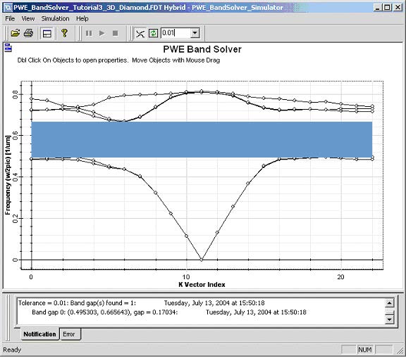
The obtained band structure of the diamond lattice clearly has a complete band gap. Click on the Locate Band Gap button on Diagram toolbar to find details on the band gap: (0.4954, 0.6656), gap=0.170.
Figure 5: Hybrid band structure of diamond lattice (mesh16*16*16)


