- Applications
Applications
Optiwave software can be used in different industries and applications, including Fiber Optic Communication, Sensing, Pharma/Bio, Military & Satcom, Test & Measurement, Fundamental Research, Solar Panels, Components / Devices, etc..
Stay up-to-date with the latest updates
- Products
Products
- OptiSystem
- OptiInstrument
- OptiSPICE
- OptiFDTD
- OptiBPM
- OptiFiber
- OptiGrating
- OptiMode
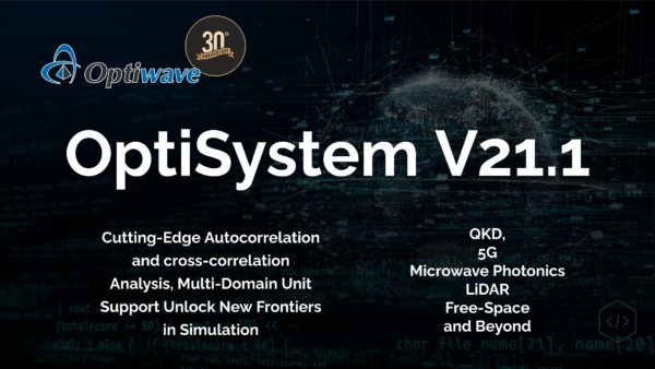
OptiSystemOptiSystem is a comprehensive software design suite that enables users to plan, test, and simulate optical links in the transmission layer of modern optical networks.
OptiInstrumentOptiInstrument addresses the needs of researchers, scientists, photonic engineers, professors and students who are working with instruments.
OptiSPICEOptiSPICE is the first circuit design software for analysis of integrated circuits including interactions of optical and electronic components. It allows for the design and simulation of opto-electronic circuits at the transistor level, from laser drivers to transimpedance amplifiers, optical interconnects and electronic equalizers.
OptiFDTDOptiFDTD is a powerful, highly integrated, and user friendly CAD environment that enables the design and simulation of advanced passive and non-linear photonic components.
OptiBPMOptiBPM is a comprehensive CAD environment used for the design of complex optical waveguides. Perform guiding, coupling, switching, splitting, multiplexing, and demultiplexing of optical signals in photonic devices.
OptiFiberThe optimal design of a given optical communication system depends directly on the choice of fiber parameters. OptiFiber uses numerical mode solvers and other models specialized to fibers for calculating dispersion, losses, birefringence, and PMD.
OptiGratingEmerging as a de facto standard over the last decade, OptiGrating has delivered powerful and user friendly design software for modeling integrated and fiber optic devices that incorporate optical gratings.
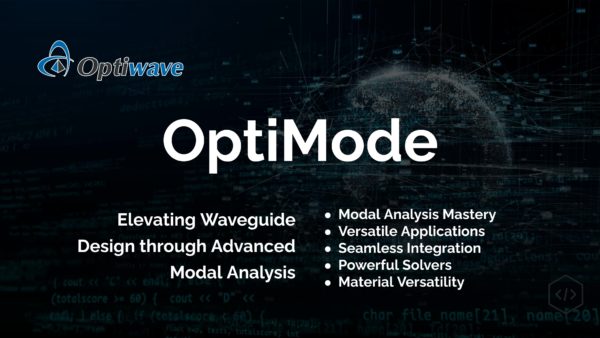
OptiModeLearn more about our products
- Downloads
Downloads
Download our 30-day Free Evaluations, lab assignments, and other freeware here.
Learn more about our 30-Day Evaluations
- Support

Want to learn more?
- Forum Login
- Applications
Applications
Optiwave software can be used in different industries and applications, including Fiber Optic Communication, Sensing, Pharma/Bio, Military & Satcom, Test & Measurement, Fundamental Research, Solar Panels, Components / Devices, etc..
Stay up-to-date with the latest updates
- Products
Products
- OptiSystem
- OptiInstrument
- OptiSPICE
- OptiFDTD
- OptiBPM
- OptiFiber
- OptiGrating
- OptiMode
OptiSystemOptiSystem is a comprehensive software design suite that enables users to plan, test, and simulate optical links in the transmission layer of modern optical networks.
OptiInstrumentOptiInstrument addresses the needs of researchers, scientists, photonic engineers, professors and students who are working with instruments.
OptiSPICEOptiSPICE is the first circuit design software for analysis of integrated circuits including interactions of optical and electronic components. It allows for the design and simulation of opto-electronic circuits at the transistor level, from laser drivers to transimpedance amplifiers, optical interconnects and electronic equalizers.
OptiFDTDOptiFDTD is a powerful, highly integrated, and user friendly CAD environment that enables the design and simulation of advanced passive and non-linear photonic components.
OptiBPMOptiBPM is a comprehensive CAD environment used for the design of complex optical waveguides. Perform guiding, coupling, switching, splitting, multiplexing, and demultiplexing of optical signals in photonic devices.
OptiFiberThe optimal design of a given optical communication system depends directly on the choice of fiber parameters. OptiFiber uses numerical mode solvers and other models specialized to fibers for calculating dispersion, losses, birefringence, and PMD.
OptiGratingEmerging as a de facto standard over the last decade, OptiGrating has delivered powerful and user friendly design software for modeling integrated and fiber optic devices that incorporate optical gratings.
OptiModeLearn more about our products
- Downloads
Downloads
Download our 30-day Free Evaluations, lab assignments, and other freeware here.
Learn more about our 30-Day Evaluations
- Support
-
Want to learn more?
- Forum Login