In the above parameter set up, if we only set one term, and set resonant frequency
as zero, we will simulate a Drude model material
| 7 | Click “Store” to save the defined material.
The “Lorentz_Drude_Al” will be listed in the FDTD-Dielectric folder of the Waveguide Profile Designer |
| 8 | In the directory under “OptiFDTD_Designer1” Profile folder, right-click the “Channel“ folder, and select New.
The “ChannelPro1” will be created and its data entry dialog box will appear. |
| 9 | In the “ChannelPro1 dialog box, set Profile Name to “ChannelPro1_Al” and 2D ProfileMaterial to “Lorentz_Drude_Al”. |
| 10 | Save the profile. |
| 11 | Close the Profile designer. |
Designing the waveguides
| Step | Action |
| 1 | In the “Initial Properties” dialog box, set the following parameters:
Waveguide Properties Width: 0.135 [mm] Profile: ChannelPro1_Al Wafer dimension Length: 1.0 [mm] Width: 0.54 [mm] 2D Wafer Material: Air |
| 2 | Click OK to start the Layout Designer.
The OptiFDTD designer window appears. Click Zoom ( “+”) to enlarge the layout. |
| 3 | From the Draw menu, select Linear Waveguide. |
| 4 | Draw the waveguide in the layout at desired the position.
The waveguide appears in the layout. Note: Click the Select tool after drawing the waveguide. |
| 5 | Double click the waveguide to edit the waveguide position and properties.
The Linear Waveguide properties dialog box appears. |
| 6 | Set the following parameters:
Waveguide start position (offset) Horizontal: 0.225 Vertical: 0.2025 Waveguide end position Horizontal: 0.625 Vertical: 0.2025 Select “Use Default” checkbox for channel thickness tapering Width: 0.135 Depth: 0.0 Profile: ChannelPro1_Al |
| 7 | Design another linear waveguide with following parameters: Waveguide start position (offset)
Horizontal: 0.225 Vertical: -0.2025 Waveguide end position Horizontal: 0.625 Vertical: -0.2025 Select “Use Default” checkbox for channel thickness tapering. Width: 0.135 Depth: 0.0 Profile: ChannelPro1_Al |
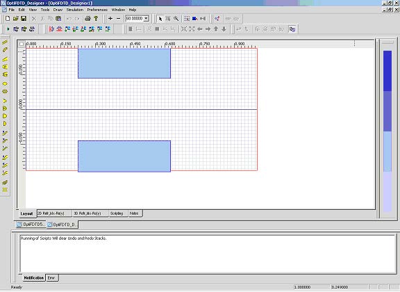
The layout will look as presented in Figure 2.
Figure 3: Waveguide in the layout
Setting the Input Plane
| Step | Action |
| 1 | From the Draw menu, select Vertical Input Plane. |
| 2 | Insert the Input Plane into the layout at the desired position.
A red line representing the input plane appears in the layout window. |
| 3 | Double-click the Input Plane.
The “Input Field Properties” dialog box appears. |
| 4 | Select Gaussian Modulated Continuous Wave radio button. |
| 5 | Set the center wavelength to 0.55um. |
| 6 | Click Gaussian Modulated CW button, and set the following parameters:
Time offset (sec): 1.0e-14 Half Width (sec): 1.0e-15 Note: This step set the time domain input as pulse |
| 7 | Click the General tab, and then click Rectangular radio button. |
| 8 | Click the 2D Transverse tab to Set the plane wave properties
Center Position: 0.0 Half Width: 0.27 Tilting Angle: 0.0 Effective Refractive Index: Local Input Amplitude or Power: 1.0 |
| 9 | Click the “General” tab, set “Plane Geometry Position” to 0.125 and select “Positive direction”. |
| 10 | Click OK to close the input plane properties dialog box. |
Setting the observation line
The observation line is only used for 2D simulations. It is used to show:
- Field distribution along the line for the user input wavelength
- Calculate the outgoing power in the line for user input wavelength
- Calculate the absolute power spectrum and normalized transmittance power spectrum (to the input power)
| Step | Action |
| 1 | From the Draw menu, select Observation Vertical Line. |
| 2 | Place the Observation Line in the desired position in the layout. |
| 3 | Double-click the observation line. |
| 4 | The “Observation Properties — Vertical Line” dialog box appears. |
| 5 | The “General” tab settings: |
| 6 | In “Center”, “Offset”, type (select) the following:
Horizontal: 0.9 mm Vertical: 0.0 mm X length: 0.54mm Label: ObservationLine1 |
| 7 | On the “Data Components” tab, select the following:
2D TE: Ey, Hx, Hz |
| 8 | Click OK. |
Setting up 2D Simulation parameters
| Step | Action |
| 1 | From the Simulation menu, select 2D Simulation Parameters.
The “Simulation Parameters” dialog box appears. |
| 2 | Select TE polarization option. |
| 3 | Set x-direction mesh and z-direction mesh to 0.005. |
| 4 | Click Advanced. |
| 5 | Set the Anisotropic PML boundary condition parameters:
+x: PMC -x: PMC +z: Anisotropic PML -z: Anisotropic PML Number of Anisotropic PML layers: 25 Theoretical Reflection Coefficient: 1.0e-12 Real Anisotropic PML Tensor Parameter: 5.0 Power of Grading Polynomial: 3.5 Note: The x- edge is set as PMC because we perform the simulations on a periodic cell and use the plane wave excitation. It works like a symmetric boundary. Please refer to the Technical Background for Plane wave simulation boundary. Please refer to the Technical Background for Plane wave simulation |
| 6 | Click Calculate to get the Time Step Size. |
| 7 | Set Run for 6000 time steps for finalization. |
| 8 | From the “Key Input Plane” drop-down list, select “Input Plane1” and “Wavelength” equal to 0.55.
Note: The Key Input Plane’s Center Wavelength will be used for the DFT calculation. |
| 9 | Click OK to close the Simulation Parameters dialog box without running the simulation, or click Run to start the OptiFDTD Simulator. |
Performing the simulation
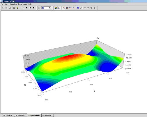
When the Simulator starts, the propagation field can be observed as presented in
Figure 4.
Figure 4: Dynamic field pattern in OptiFDTD simulator
Performing data analysis
After the simulations are completed, you can open the analyzer to do the post simulation
analysis. The tools for post-processing data analysis are already discussed in other lessons. In this lesson we will demonstrate usage of an observation line to extract the transmittance.
| Step | Action |
| 1 | In the OptiFDTD analyzer, select Observation Area Analysis in the tools menu. |
| 2 | Click Observation Line button. Observation line page appears.
This page can show the field pattern in observation line for user specified wavelength. |
| 3 | Click “Power Spectrum” button, and set the following parameters to extract the power transmittance.
Minimum wavelength: 0.4 [mm] Maximum wavelength: 1.1 [mm] Sample point: 71 Normalized with: Input Plane1 |
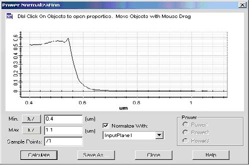
| 4 | Click “Calculate” button to start transmittance calculation. The results will be shown in the graph. (see Figure 5)
Note: It will take a while for this calculation to complete, because DFT is calculated for each field component of each point in the line calculated for each field component of each point in the line. |
Figure 5: Power normalization (Transmittance)


