
Home › Forums › SYSTEM › RF signal Modultion response (Graph Between Amplitude and Output Optical Power)
- This topic has 24 replies, 4 voices, and was last updated 9 years, 5 months ago by
 Ibn Aziz.
-
AuthorPosts
-
-
October 23, 2014 at 3:12 pm #14494
 Ibn AzizParticipant
Hi ever one
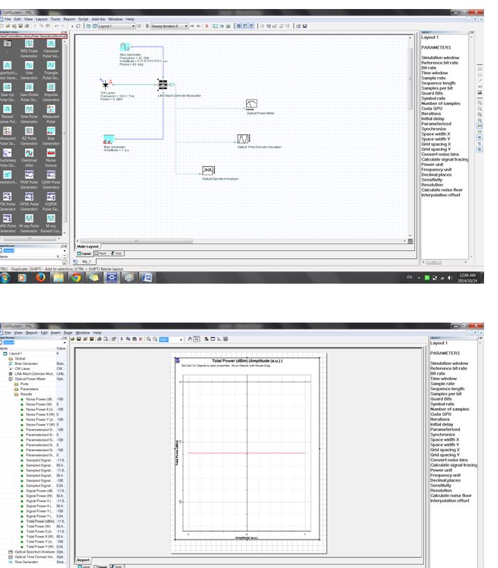
I am trying to modulate RF signal using LiNb Modulator and Dc bias as shown in below figure (i have taken default values).
But the problem is that when i want to make 2-D graph between RF input signal(the input RF signal amplitude is sweep between -1 to 1 for
10 iterations) and modulator output optical power measured from power meter. The 2-D graph between them gives constant value (i am also
attaching the same constant curve) also Optical power meter shows same measured reading throughout (-1 to 1 sweep iterations values of)
input RF Signal.
(In the graph RF signal amplitude is on X-axis while Modulator Out power on Y-axis)
So i want to know
1. why it behaves like that ?
2. and modulator output power should change with input voltage but that is not happening here, why ?
3. how can we make output power of modulator change with input RF Signal ?
4. Kindly share any tutorials related to such RF modulation using DC biasing or any RF modulation related tutorials ???
i am working on it since last week but couldn’t find any solution.
i will be v thankful to u for ur kind help and response.
BEST REGARDS
BEST WISHES
Attachments:
-
October 23, 2014 at 3:59 pm #14498
 Jaffar Emad KadumParticipant
Dear Bilal;
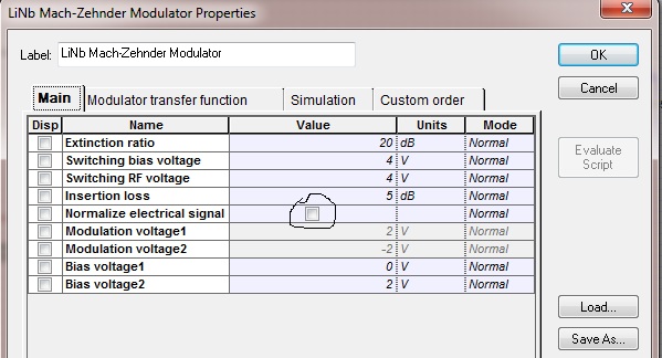
Your modulator may be set the electrical input as ( NORMALIZED), so the modulator take the input voltage (one) for all iterations. Other cases, for intensity modulation you must work in quadrature point of transfer function of the modulator and this done be controlling the bias voltage and amplitude of the electrical input.
Jaffar
-
October 23, 2014 at 4:36 pm #14501Ibn AzizParticipant
Dear Jaffar Thanks for ur kind response.
1. Your modulator may be set the electrical input as ( NORMALIZED), so the modulator take the input voltage (one) for all iterations.
So how can i change this ? and make my system work properly ??
2. Other cases, for intensity modulation you must work in quadrature point of transfer function of the modulator .
I didn’t got this point.
Can u share any references related to them so that i can approach and make my grip over them ??3. this done be controlling the bias voltage and amplitude of the electrical input.
i tried many time by changing bias Voltag and also electricl signal amplitud but stil same result.
plz if u have some refrences kinldy share , i wil be very thakful to u.
Best Regards
Best wishes -
October 23, 2014 at 4:39 pm #14502Ibn AzizParticipant
Dear Jaffar one more help plz and @all ..
I want to know how to find the “Time period and pulse width” of the generated output modulated optical
signal from the above setup ?I want to know/measure these parameters through Opti system softwre tool or any othr procudere e.g. As we use power meter to measure output power similarly is there any procedure for measuring Time Perid and pulse width of Generated output optical signal ??
Please share.
I will be very thankful to u, for ur this kindness.
Best Regards
Best Wishes -
October 23, 2014 at 5:25 pm #14505Jaffar Emad KadumParticipant
Dear Bilal,
you can change the modulator setting through component properties as attached. I think, although when you change the amplitude of the electrical input the power still constant. As we know the MZM modulator has man modes of operation including quadrature point, null point and maximum point and there is a specific setting for each operation. I attached you here a file I got it from this forum includes different modulator setting.I use the markers in the visualizers to measure the pulse width.
Hope this help
Thanks
-
October 23, 2014 at 11:54 pm #14512
Ravil
ParticipantHi bilalaziz, you move your operating point to quadrature point of transfer function of the modulator by including a 90-degrees phase shift in MZM arm. I corrected this issue in one of my schemes by doing that.
-
October 24, 2014 at 2:37 am #14520Ibn AzizParticipant
Thanks Alot Ravi and jaffar
Can u share any tutorial or research paper related to quadrature point, null point and maximum point operation of MZM or any thing related to these operations setup or explanation or any book ??
I have searched alot but couldn’t find any thing sold related to Modulation approaches.
I am very thankful to u for ur precious effort.
Best Regards
Best WIshes-
October 24, 2014 at 9:40 am #14527
Damian Marek
ParticipantHey bilalaziz,
Jaffar had a good suggestion with the file he attached. It shows a quick example of different bias operating points. There is also a post in our knowledge section that may clarify parts:
Regards
-
-
October 29, 2014 at 5:28 pm #14686Ibn AzizParticipant
Q. Damian Marek I have done detail analysis of the file that u have shared on above mentioned link but I need some more assistance from u in rectifying some unsolved ambiguities .
For Peak Operating Point u have taken these parameters and values
i.e
Bias (Vdc=0); V1-V2=0
Vpi=4; Vrf=4
Max Voltage delta is 4(Vpi)So I want to know …
1. What “Peak Operating Point” is referring to?
2. How u relate all these above parameters that u have describe with each operation point ( Peak Operating point, Null Operating point and Quadrature operating point ) with Sine generator and MZM modulator?
3. Further i want to know, how and why u has chosen all these values ?
4. And how these values and parameters affect the operation of all three different operations??
Similarly for Quadrature operating point and Null operating point. There parameters with value from attached file is as under
a. Quadrature operating point
Bias (Vdc=Vpi); V1-V2=Vpi/2=2
Vpi=4;Vrf=4
Max Voltage delta is 4(Vpi)c. Null operating point
Bias (Vdc=Vpi); V1-V2=Vpi=4
Vpi=4;Vrf=4
Max Voltage delta is 8(2Vpi) -
October 30, 2014 at 10:12 am #14699Participant
Hi bilal,
Good questions!
1) The operating point is really just the DC bias between the two branches of the modulator and thus the optical phase difference between the two branches. The first example is named the peak operating point because the DC bias is 0, and so the optical phase difference between the two signals is 0. This is constructive interference so the operating point (DC) is said to be at its peak value. Null operating point is when the phase shift is PI and the quadrature operating point is at PI/2.
2) I think this is answered in my above response if you take into consideration the electrical gain component with a value of -1 will in effect double whatever bias the sine generator is set with. Think about a reflection of the electrical signal across the x axis.
3) Using the Vpi value of 4V these bias points can be calculated. Remember that Vpi is the required voltage difference between the branches to induce a phase shift of PI. Naturally the bias voltage for the Null operating point should be 4V and the bias voltage for quadrature operating point is (Pi/2)/Pi = Vb/Vpi Vbias = 2.
The Vrf component property is used if you want to decompose your input signal into DC and AC. In this case the Vrf will act as the Vpi for the AC signal. I suggest looking at the technical background for this component for more in depth explanation. Double-click->Help
4) Depending on where the bias point is and how large your input AC amplitude is you can make different pulse shapes. The objective of this example file was to demonstrate this fact. The technical background explicitly shows the equation used to calculate the output optical waveform from the electrical signals.
I hope this clears things up!
-
October 30, 2014 at 5:15 pm #14714Ibn AzizParticipant
Thanks alot Damian Marek.
but i need some more clarification from ur side, i hope u wil help.
1. As we are not using any DC Generator in the setup So why u have used the word “DC Bias” at many places above? or why we say it Dc bias ?
2. why are we biasing sine generator at 0 for peak operating point and at 2 for zero operating point and at 1 for Quadrature operating point ?
3a. When we are giving -1 electrical gain to sine generated signal so its phase changes, But when signal from sine generatr and othr from electrical gain goes into modulotr then what process is responsible for generation of output optical signal aftr MZM modulatn.
As both sine generated signal and electricl gain signal are out of phase SO they must cancel each othr behavior but they don’t.SO what process is going on inside MZM modultor that they are not canceling each othr ??
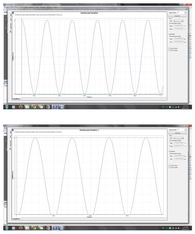
i am attaching there signal shape before entering into MZM modulator.
3b. I have taken into consideration of reflection acros x-axix of electicl gain generted signal and sin genrtd signal but how it double’s the effect, as both the signal are out of phase ??
i have also attached their graph below.4. Further Damian Marek i am very confuse and astonish that how and what processes is responsible for generation of optical pulses at the output of MZM modulator ? as at the input we are using Continuous wave laser and sin generator. SO what is going on inside MZM that results into genration of optical pulses at the oetput ??
From the help section that u have given with optisys, we couldnt’ get clear or u can say that there is no such info over ther …..
Please explain this point in detail as it is very confusing and v interesting to know about it…..
5.from above ur answer about Quadrature operation point ..
(Pi/2)/Pi = Vb/Vpi Vbias = 2.
what is Vb??1/2 =(Vb/4)(Vbias)= 2 (how we get 2)
Attachments:
-
October 31, 2014 at 9:37 am #14729Participant
Hello,
1) The Sine generator actually has an option for creating a bias and if you look closely at the graphs attached you can see that the signal is biased. DC is a term from electronics (I guess it doesn’t really have a place here!), which means direct current. This is a another way of saying the time independent part of your signal. DC bias and bias are really the same.
2) You might want to look at a textbook or maybe look around on the web to get a good theoretical description of how modulators function, but I’ll give it a shot with a couple of words. An electrical field (voltage) can affect the index of refraction of a material. In a modulator, the optical signal is split into two equal beams and propagated through their own waveguide. Controlling the voltages on each arm independently it is possible to create a phase shift between the two optical signals by changing the index of refraction (phase velocity).
The Vpi is the necessary voltage to cause a pi phase shift on an incident optical signal. So if you keep one branch at 0 V and you apply a Vpi voltage on the other branch the optical signal will interfere destructively at the output.
http://en.wikipedia.org/wiki/Electro-optic_modulator
4) For my calculations Vb is the Vbias and it wasn’t supposed to be part of the equation, sorry about that.
Hope this is more clear now!
-
October 31, 2014 at 9:49 am #14730Ibn AzizParticipant
Thanks alot Damian Marek.
-
October 31, 2014 at 9:54 am #14731Ibn AzizParticipant
Hi Damian Marek,
Hope u r in gud health
Sir kindly explain this point also
how and what processes is responsible for generation of optical pulses at the output of MZM modulator ? as at the input we are using Continuous wave laser and sin generator. SO what is going on inside MZM that results into genration of optical pulses at the output ??
Best regards
Best Wishes-
October 31, 2014 at 12:51 pm #14740Participant
This is partly answered in my response, I just grouped it in with answer 2. I’m having a hard time finding a good reference on the web that explains clearly how a mach zehnder modulator works. But basically it comes down to splitting an optical signals into 2 branches and inducing a phase shift in one of them via an electrical signal. Higher voltage means a higher phase shift is induced. When the two signals are combined again they can experience constructive or destructive (or anything in between) interference.
Regards
-
-
October 31, 2014 at 6:36 pm #14748Ibn AzizParticipant
Damian Marek thaks alot sir. i am very thankful to u.
Best Regards
Best Wihses -
October 31, 2014 at 10:33 pm #14760Ibn AzizParticipant
hello Dear Damian Marek !
hope u r fine!
As in above comments of Ravil and Jaffer Emad states that “Why we need to work in Quadrature point of transfer function for intensity modulation of MZM” ?
So i need to know y we need to work in ths point of operation ? we can achive intensity modulation by Null point operation. Because of pi phses shift introduce during its operation.
Am i corresct ?
Any one among u, who know the correct answer/idea among u plz share ur knowledge.
i will we very thakful to u for ur kind support and help
Best regard
Stay bless-
November 3, 2014 at 9:54 am #14783Participant
There is no reason why you would have to operate at the quadrature point. The only reason is that operating at different bias points changes the type of pulse generated in the mach zehnder modulator. The null point can be used as well.
Edit: I should fix this to say that there IS a reason for choosing different bias points. Usually it has to do with the desired shape of the pulse.
-
-
November 3, 2014 at 10:12 am #14786Jaffar Emad KadumParticipant
Usually, We bias MZM at quadrature point in Direct detection system and at null point in Coherent detection system.
-
November 6, 2014 at 8:32 pm #15046Ibn AzizParticipant
Thanks Jaffar for ur kind response.
Regards
Stay Bless -
November 6, 2014 at 8:46 pm #15048Ibn AzizParticipant
@all
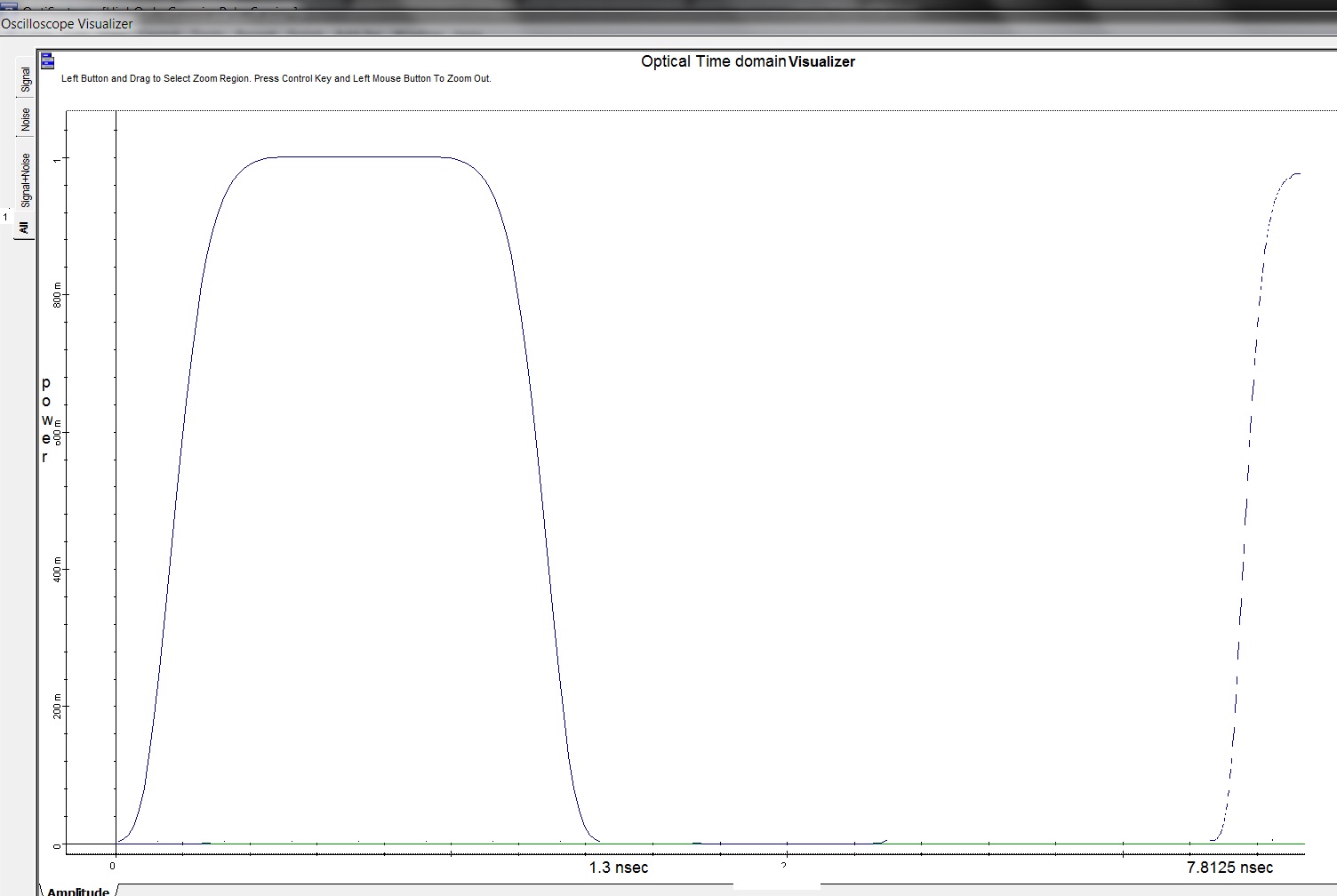
I am working on a project in which i require pulse shape signal from continuous wave source signal. The configuration of required pulse is attach as follow and fig is attached below.
Time period of optical pulses = 7.8125 nsec
pulse width of optical pulses = 1.3 nsecI have used all above operation points but couldn’t make it posible.
Now the problem is that i get required Time period and some configuration then the required pulse width couldn’t obtainable vice versa.
if u have any idea or apprach to get this typ of pulse from Contineuos source plz share.
I wil be very thakful to u for ur this act of kindness.
Best regards
Stay BlessAttachments:
-
November 7, 2014 at 1:27 pm #15090Participant
Can you send your most recent project file over? The time period pretty much sets your bit rate so at least that is one constraint out of the picture. I haven’t done much pulse shaping with cascaded MZM’s, but I might be able to fix your project file.
-
November 10, 2014 at 11:41 pm #15171Ibn AzizParticipant
Thanks Damien Marek for ur kind response.
Damien i have done with the project and really very thankful to u for ur kind help and suggestion.
May God bless u .
Best Regards
Best Wishes -
November 11, 2014 at 9:42 am #15206Ibn AzizParticipant
Damien marik one more thing if u want to know hw i did that then kindly visit this link, here i have attached the file name “EAM_Scenario”.
link:
Best Reagrds
Best Wishes -
November 11, 2014 at 3:30 pm #15211Ibn AzizParticipant
Damien marik !
if u resolve one more problem at above given link then it wil be highly appreciable.
Best Regards
-
-
AuthorPosts

- You must be logged in to reply to this topic.