Applications
- Design and simulation of opto-electronic circuits at the transistor level
- Signal integrity analysis of opto-electronic circuits
Benefits
- Offers greater ease of schematic capture, parameter specification, waveform probing and usage.
- State-of-the-art transient time domain, small-signal frequency, and noise analysis to accurately predict behaviour of advanced opto-electronic circuits.
- Waveform analysis using OptiSystem for complex post- processing functionality. Advanced visualization tools produce OSA Spectra, signal chirp, eye diagrams, polarization state, constellation diagrams and much more.
- Includes parameter extraction tools for OptiSPICE model creation. From measured data, parameter extractors are used to find optimal model parameters to fit the measurement.
Simulation Description
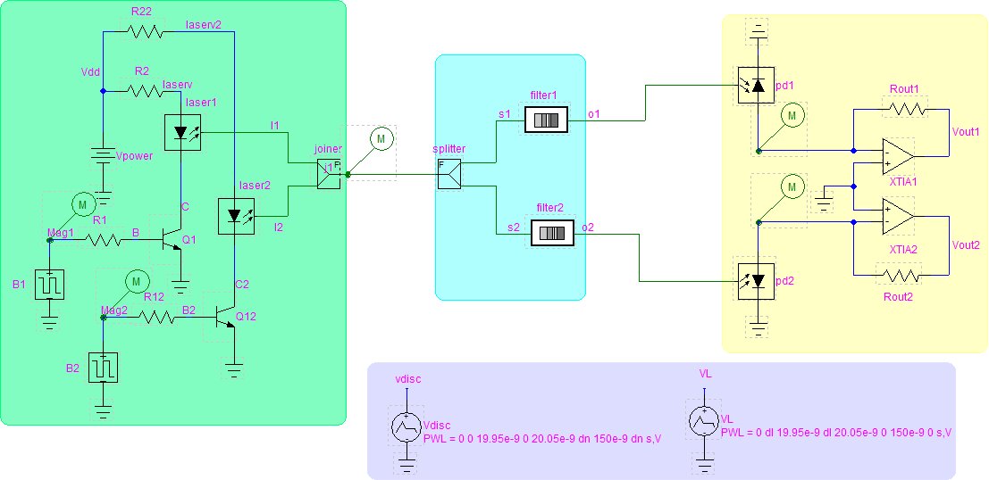
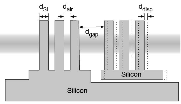
In the above opto-electronic circuit, we have simulated the switching between two optical channels (193.1 THz and 192.75 THz) at the receiver end of the system by using active MEMS filters. The physical structure of the MEMS based filter is presented in the figure below. The filter consists of three elements: two Bragg diffraction mirrors formed by alternating layers of Silicon (N = 3.5) and Air (N = 1.0) and central air gap that can be changed in size by moving one of the mirrors. The active filter is implemented using the Multi-layer Filter – Explicit component that allows voltage dependent indices for all layers.
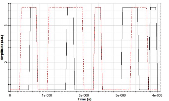
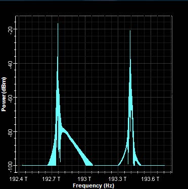
The following results show a 40ns transient simulation for the opto-electronic circuit. The top plot shows the two input bit-streams for the two channels (black line – channel1, red line – channel 2) that are initially transmitted. The next plot shows the multiplexed optical channels spectrum before the splitter component.
The displacement in the filters dgap was modified in time by controlling the voltage Vd and VL to create a linear transition in the filter characteristics. Filter 1 initially selects the data stream from channel 1. At t ![]() 20 ns the control voltage is changed in a way such that the optical channel 2 is selected. The inverse procedure happens to filter 2, where it initially selects channel 2, and at t = 20 ns it switches to channel 1.
20 ns the control voltage is changed in a way such that the optical channel 2 is selected. The inverse procedure happens to filter 2, where it initially selects channel 2, and at t = 20 ns it switches to channel 1.
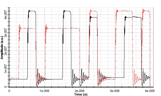
The bottom graph shows the bit streams received by the upper receiver branch (black line) and by the lower receiver branch (red line). From the graph, we notice that
the upper receiver detects the initial data stream from channel 1, and in the middle it starts to detect the data stream from channel 2. In the lower receiver, the data
stream from channel 2 is initially detected and in the second half channel 1’s data is received.