
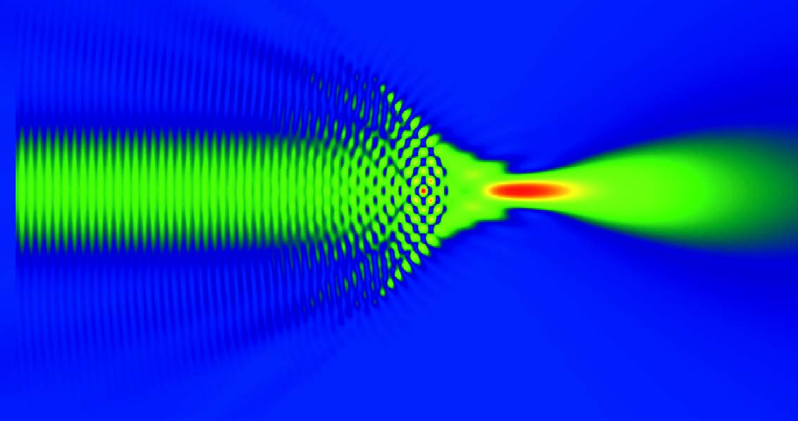
OptiFDTD enables you to design, analyze and test modern passive and nonlinear photonic components for wave propagation, scattering, reflection, diffraction, polarization, and nonlinear phenomena. The core program of OptiFDTD is based on the finite-difference time-domain (FDTD) algorithm with second-order numerical accuracy and the most advanced boundary condition – the uniaxial perfectly matched layer (UPML) boundary condition. The algorithm solves both electric and magnetic fields in temporal and spatial domains using the full-vector differential form of Maxwell’s coupled curl equations. This allows for arbitrary model geometries and places no restriction on the material properties of the devices. OptiFDTD dramatically improves the productivity of design engineers by reducing time-to-market.
APPLICATIONS
- Dielectric and metallic gratings
- CMOS sensors design
- VCSEL lasers passive design
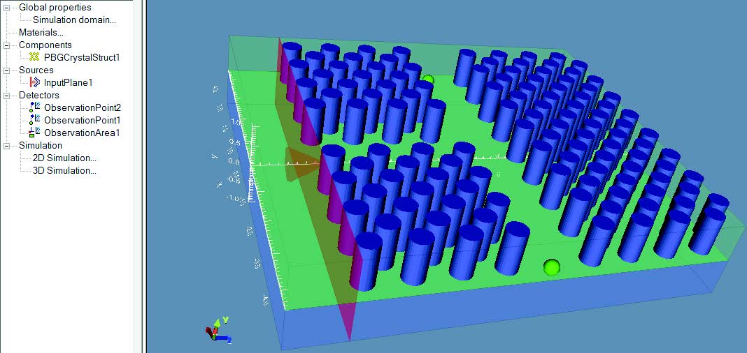
- Photonic crystals
- Integrated optics
- Optical filters and resonators
- Solar cells
- LED and OLED passive design
- Nanolithography
- Plasmonics
- Surface Plasmon Resonance
- Nanoparticles simulations
- Diffractive micro-optics elements
- Tissue scattering simulations
KEY FEATURES
Integrated simulation environment
OptiFDTD provides a complete and user-friendly 3D graphical user interface to enable the design, simulation, and analysis of complex devices. Designs from third-party CAD software can be readily imported and exported using widespread formats such as DXF and GDSII. OptiFDTD and OptiBPM can easily interoperate to extend the simulation range attainable by OptiFDTD alone.
Powerful automation and parameter sweeps
OptiFDTD designs and simulations can be fully automated using a powerful Visual Basic scripting language. The language is easy to learn and provides standard programming structures such as objects, loops, and tests. Parameter sweeps provide an easy-to-use graphical interface for defining parametric simulations, where one or two parameters vary at each iteration. OptiFDTD post-processing tools can take advantage of automation functionalities and assist you in optimizing your design.
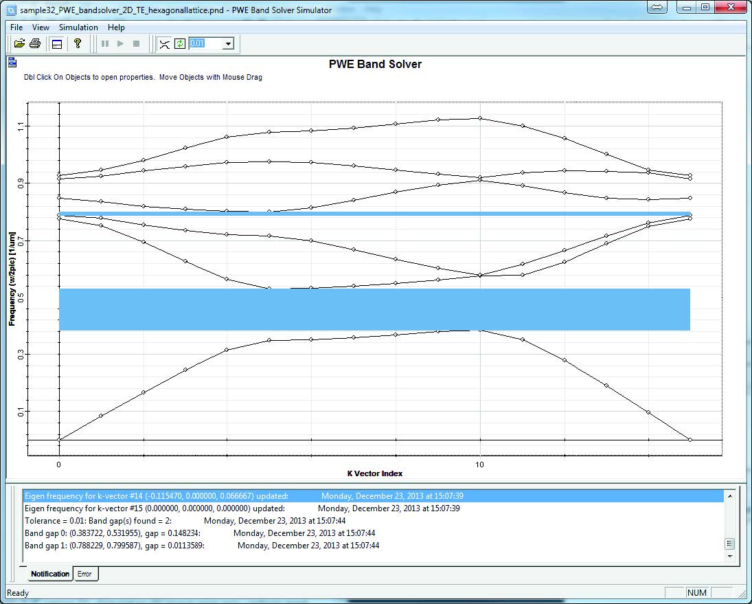
Plane Wave Expansion band solver for photonic crystals
A fully integrated 2D PWE band solver and photonic crystal editor can help you design and simulate any type of photonic crystal problem (1D, 2D, 3D). The PWE band solver can scan through k-space following the irreducible Brillouin zone and find eigenfrequencies of your structure. Band gaps are automatically outlined in the resulting band diagram.
True parallel performance
OptiFDTD takes advantage of modern 64-bit operating systems and processors. It is optimized to run efficiently on multiple cores and processors in a single machine using shared memory, providing the best possible performance and minimum memory footprint (as compared to distributed memory architectures such as MPI). For memory intensive simulations, you can use our Linux 3D simulation engine, specifically designed to take advantage of Linux computer clusters.
“We are using OptiFDTD to perform 2D and 3D simulations of CMOS image sensor pixels to evaluate their optical effciency. OptiFDTD is a very versatile simulation tool and we have been very impressed with the technical support we have received from Optiwave.”
Dr. Peter Catrysse
Dept. of Electrical Engineering,
Stanford University
Advanced simulation post-processing tools
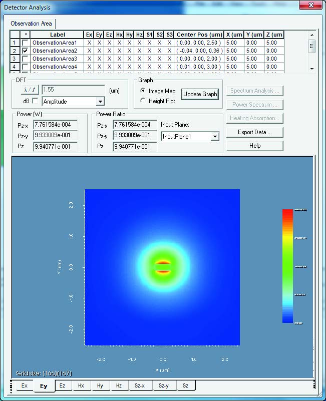
OptiFDTD provides extensive simulation analysis tools. Using OptiFDTD Analyzer, you can observe the time domain and frequency domain (using FFT or DFT transforms) amplitude, phase, real or imaginary values of any field component recorded by your detectors. All field data can be exported to third-party software tools such as Matlab™ or Origin™ for further processing or publication. Time-domain field evolution can also be visualized in the form of movies. Polarized power distribution, Poynting vectors, overlap integrals, heat absorption calculation, and far-field transforms can be determined using OptiFDTD Analyzer and OptiFDTD Toolbox.
Sources:
- Waveguide mode input using OptiMode
- Gaussian beam input
- Plane-wave
- Point source (dipole)
- Single wavelength (CW) source
- Pulsed source
- Linear or circular polarizations
- Simulation of multiple sources simultaneously
Materials:
- Dielectric (lossless and lossy) material, (n,k) direct entry, or Sellmeier model for glasses
- Isotropic or anisotropic media
- Dispersive (Lorentz, Drude and Lorentz-Drude)
- Nonlinear media (2nd, 3rd order, Kerr and Raman)
- Perfect conductor material
- Extensive Material Library
Boundary conditions:
- Uniaxial Perfectly Matched Layers (UPML)
- Perfect Electric Conductor (PEC)
- Perfect Magnetic Conductor (PMC)
- Periodic Boundary Conditions (PBC)
Geometry:
- Straight and titled waveguides with taper function
- Ring, arc, circle, and ellipse waveguides with taper
- Parabolic and exponential waveguides with taper
- 3D shapes with clipping functions
- Photonic crystal lattice editor
- Import from 3rd party CAD layout software
- Export masks for lithography
Simulator:
- 2D TM or TE, 3D simulations
- Non-uniform meshing capabilities
- PWE band solver for photonic crystals
- Full 64-bit simulation, Multithreaded engine
- Cluster computing: hybrid multithreading / MPI engine on Linux clusters
Detectors and Post-processing:
- Point detector (temporal and spectral)
- Line and area detectors (DFT spectra)
- Mode analysis
- Poynting vector analysis
- Polarized power analysis
- Far-field transform
- Fields exported to text, images, or movies

