
Lorentz dispersive material currently can only be simulated in 2D. This lesson describes how to create, run, and analyze a Lorentz dispersive material simulation.
The corresponding layout file is available in the sample folder of OptiFDTD:
Sample06_2D_TE_Multi-Lorentz_Dispersion_Multi-Input.FDT.
The corresponding results file is available on the OptiFDTD setup CD:
Sample06_2D_TE_Multi-Lorentz_Dispersion_Multi-Input.FDA.
Creating a layout
| Step | Action |
| 1 | Open Waveguide Layout Designer. |
| 2 | To create a new project, from the File menu, select New.
The Initial Properties dialog box appears. |
| 3 | To open the Profile Designer and set up the material and profile, click
Profiles And Materials. The Profile Designer opens. |
| 4 | In the directory under OptiFDTD_Designer1, under the Material folder, right- click the FDTD-Dispersive folder.
A context menu appears. |
| 5 | Select New.
The FDTDDielectric1 material definition dialog box appears. |
| 6 | In the FDTDDielectric1 material definition dialog box, click Lorentz Dispersive.
The Lorentz Dispersive dialog box appears (see Figure 1). |

Figure 1: Lorentz Dispersive
| 7 | Select Lorenz Dispersive, and define the following parameters:
Name: FDTD_Lorentz_res3 ε∞ (F/m): 1.630130e00 ε0 (F/m): 2.630130e00 Resonance number: 3 |
| 8 | Click Sellmeier Equation and input the corresponding values in the Sellmeier Equation table shown in Figure 1. |
| 9 | Click Transform To Lorentz Model, then click Lorentz Model radio button.
The Lorentz model resonant frequency, damping factor, and strength are shown in Figure 2. |
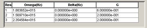
Figure 2: Frequency, damping factor, and strength
| 10 | Click Store to save the material. |
| 11 | Repeat Step 4 to design a linear material with refractive index equal to 2.1 and the material with the name FDTDDielectric2.1, and click Store. |
| 12 | In the directory under Profile Designer, under the Profile folder, right-click the Channel folder.
A context menu appears. |
| 13 | Select New.
The ChannelPro1 dialog box appears. |
| 14 | In ChannelPro1 dialog box, set the Profile Name as Lorentz_res3 and the 2D profile material as FDTD_Lorentz_res3. |
| 15 | Save the profile. |
| 16 | Repeat Steps 12 to 14 design another 2D channel profile with the name Linear2.1 and the material as FDTDDielectric2.1. |
| 17 | Click Store to save the defined profile. |
| 18 | Close the Profile Designer. |
| 19 | In the Initial Properties dialog box, set the following parameters:
Waveguide Properties Width: 1.0 Profile: Lorentz_res3 Wafer dimension Length: 10 Width: 8 2D Wafer Material: Air |
| 20 | Click OK to start the layout designer.
The Designer window appears. |
| 21 | In the Waveguide Layout Designer window, from the Draw menu, select Linear Waveguide. |
| 22 | Draw the waveguide in the layout at the desired position.
The waveguide appears in the layout. |
| 23 | To edit the waveguide position and properties, double-click the waveguide in the layout.
The Linear Waveguide Properties dialog box appears. |
| 24 | Type the following parameters:
Waveguide start position Horizontal: 0 Vertical: 2 Waveguide end position Horizontal: 10 Vertical: 2 Select the Use Default checkbox. Width: 1.0 Depth: 0 Profile: Linear2.1 |
| 25 | Repeat Steps 21 to 23 design another linear waveguide with following properties:
Waveguide start position Horizontal: 0 Vertical: –2 Waveguide end position Horizontal: 10 Vertical: –2 Select the Use Default checkbox. Width: 1.0 Depth: 0 Profile: Lorentz_res3 The two waveguides appear in the layout. The upper one is the Linear waveguide, and the lower one is the Lorentz Dispersive waveguide (see Figure 3). |

Figure 3: Linear and Lorentz Dispersive waveguides
Setting the Input Plane
| Step | Action |
| 1 | From the Draw menu, select Vertical Input Plane. |
| 2 | Click in the layout to place the Input Plane in the desired position.
A red line that presents the input plane appears in the layout window. |
| 3 | To edit the Input Plane properties, in the layout, double-click the Input Plane.
The Input Field Properties dialog box appears. |
| 4 | Click Gaussian Modulated Continuous Wave. |
| 5 | Set the center wavelength to 1.35um |
| 6 | To edit the Input Pulse, click the Gaussian Modulated CW tab. |
| 7 | Type the following values:
Time offset (sec): 4.0e-14 Half width (sec): 1.5e-14 |
| 8 | Click the General tab, and then click Modal. |
| 9 | Click the 2D Transverse tab to start solving the 2D TE fundamental mode for the lower waveguide, and then apply the solved mode as the input plane. |
| 10 | Repeat Steps 1-8 to design another vertical input plane in the same position as Input Plane1, and set the Mode input for the upper waveguide. |
Setting up the Observation point
| Step | Action |
| 1 | From the Draw menu, select Observation Point. |
| 2 | Click in the layout to place the observation point in the desired position. |
| 3 | To edit the observation point properties, double-click the observation point in the layout.
The Observation Point Properties dialog box appears |
| 4 | Type the following values:
Center Position Horizontal: 7.5um Vertical: –2 Depth: 0 Data Components 2D TE: Ey (default) |
| 5 | Repeat Steps 1 to 4 to design another observation point with the following values:
Center Position Horizontal: 7.5um Vertical: 2 Depth: 0 Data Components 2D TE: Ey (default) |
Setting up the 2D simulation parameters
| Step | Action |
| 1 | From the Simulation menu, select 2D Simulation Parameters.
The Simulation Parameters dialog box appears (see Figure 4). |

Figure 4: Simulation Parameters dialog box
| 2 | Click TE. |
| 3 | Type the following Mesh Delta X and Mesh Delta Z values: 0.05 |
| 4 | To set the Anisotropic PML boundary condition parameters, click Advance.
The Boundary Conditions dialog box appears. |
| 5 | Type the following values:
Number of Anisotropic PML layer: 10 Theoretical Reflection Coefficient: 1.0e-12 Real Anisotropic PML Tensor Parameter: 5.0 Power of Grading Polynomial: 3.5 |
| 6 | Click OK. |
| 7 | Click Calculate for time step size. |
| 8 | In the Run for Time Steps (Results Finalized) field, type 3000. |
| 9 | From the Key Input Plane drop-down list, select Input Plane1 and wavelength:1.35
Note: The Key Input Plane center wavelength is used for the DFT calculation. |
| 10 | To save the settings and start the 2D simulation, click Run. |
| 11 | After the simulation ends, open OptiFDTD_Analyzer. |
Performing the simulation
| Step | Action |
| 1 | In OptiFDTD_Simulator, view the refractive index distribution and the wave propagation (see Figure 5). |

Figure 5: View simulation results in OptiFDTD_Analyzer
| Note:
– The two input waves have the same parameters. – The wave in the Dispersive waveguide is delayed because of the Dispersive effect. |
|
| 2 | To view the dynamic time domain and frequency domain response, from the View menu in the OptiFDTD_Simulator, select Observation Point Analysis.
The Observation Area Analysis dialog box opens (see Figure 6). |

Figure 6: Observation Area Analysis dialog box
Performing data analysis
Using this example, you can perform the following analysis in OptiFDTD_Analyzer.
| Step | Action |
| 1 | View the layout, refractive index, Poynting vector, and field propagation pattern (DFT results) for the center wavelength (see Figure 7). |

Figure 7: View simulation results for the center wavelength
| 2 | To view the Mode Analysis, from the Tools menu, select Crosscut Viewer.
The X-Z Cut Visualizer dialog box appears (see Figure 8). |

Figure 8: X-Z Cut Visualizer dialog box
| 3 | To start the observation point analysis, from the Tools menu, select Observation Area Analysis.
The Observation Area Analysis dialog box opens (see Figure 9). |

Figure 9: Observation Area Analysis dialog box