This lesson is designed to familiarize you with the OptiFDTD layout designer concept.
The same basic steps need to be followed to layout any device in OptiFDTD. This
document will guide you through these steps and provide you with a detailed
explanation.
OptiFDTD comes as 4 main applications:
- Layout Designer – This is where you define your structure and simulation conditions.
- Profile Designer – This is used to define the materials and profiles used in the simulation.
- Simulator – This program loads the designer file and performs the simulation. The simulator is started from the layout designer.
- Analyzer – This program is used to view the results and perform some post processing. As soon as the simulation is done, the simulator will ask if you would like to open the analyzer.
This document focuses on using the layout designer. To start an OptiFDTD project,
your first step will be to open up the layout designer. From here the process of defining a layout begins.
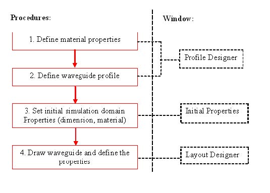
Figure 1 is a flowchart that illustrates the main steps for building a layout.
Figure 1: Flowchart for building a Layout
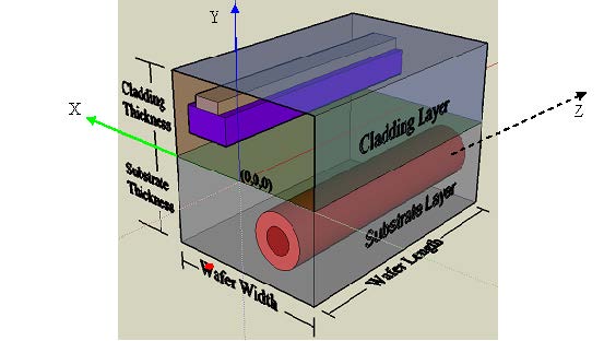
The simulation domain can be 2D (finite xz-area) or 3D (xyz-volume) depending on
the simulation that you choose. For 3D simulations, the domain is divided into 2 parts
called substrate and cladding for historical reasons. The boundary between substrate
and cladding define y = 0. Structures such as waveguides and lenses are placed
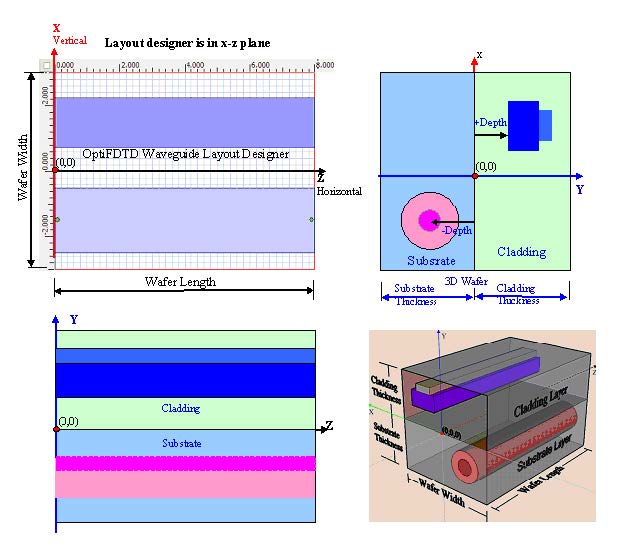
within this domain. An example layout to illuminate the design concept is illustrated in
Figure 2. We can see the substrate is the volume defined by y < 0 and the cladding
is the volume defined by y > 0. The substrate and cladding each have a material
associated with them. They define the default background material that other
structures are imbedded in. There is a channel waveguide consisting of two
rectangular layers; it is suspended in the cladding volume and extends along the z-direction. Another fiber waveguide consisting of two circular fiber layers is imbedded
in the substrate and also extends along z-direction.
The cross-sections of the rectangular waveguide and the fiber are what we call
profiles. By combining profiles with waveguide that are drawn in the layout, we can
define 3D shapes in the simulation domain.
The following is the relevant data for this layout
1)Material that will be used in the project
- Substrate material: n=2.0
- Cladding material: n=1.0 (Air)
- Material for channel waveguide layer 1: n=3.0
- Material for channel waveguide layer 2: n=2.5
- Material for fiber waveguide core layer: n=3.0 ( same as channel waveguide layer 1)
- Material for fiber waveguide cladding layer: n=2.5 ( same as channel waveguide layer 2)
2)Waveguide profile (waveguide cross section) and material
-
- Channel profile
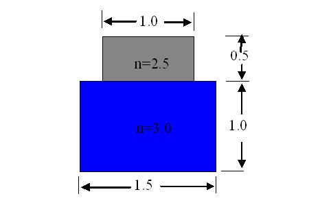
- Layer 1: width: 1.5μm; thickness: 1.0μm; Material: n=3.0
- Layer 2: width: 1.0μm; thickness: 0.5μm; Material: n=2.5
-
- Fiber profile
- Core layer: radius: 0.5μm ; Material: n=3.0
- Cladding layer: radius: 1.0μm; Material: n=2.5
3)Simulation domain properties.
- Length: 8μm (z-direction: 0μm→+8μm);
- Width : 6μm (x-direction: -3μm→+3μm)
- Substrate layer thickness: 3μm (y-direction: -3μm→0 μm), material: n=2.0
- Cladding thickness: 3um (y-direction: 0 μm→3μm), material: n=1.0 (Air)
4)Waveguide properties
-
- Channel waveguide
- Position: (1.5, 1.0, 0) μm → (1.5, 1.0, 8) μm
- Width: 1.5 μm; Thickness: 1.5 μm
-
- Fiber waveguide
- Position: (-1.5, -1.5, 0) μm → (-1.5, -1.5, 8) μm
- Width: 2.0 μm
Figure 2: Example Layout
The following detailed steps are used to build the project layout demonstrated in
Figure 2.
| Step | Action |
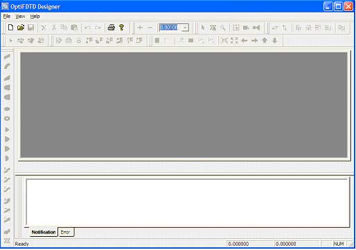
| 1 | Open OptiFDTD Waveguide layout Designer From the Start menu, select Programs >Optiwave Software > OptiFDTD > Waveguide Layout Designer. OptiFDTD_Designer window opens |
Figure 3: OptiFDTD Designer (No layout)
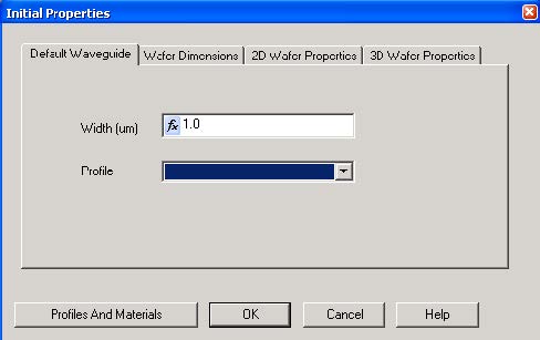
| 2 | Create a new project From the OptiFDTD_Designer File menu, select New. The Initial Properties dialog box appears. |
Figure 4: Initial Properties
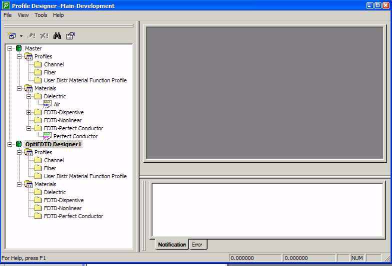
| 3 | Start Profile Designer To define the material(s) and waveguide profile(s) that will be used in the project, Click Profiles and Materials button in Initial Properties Dialog. The Profile Designer OptiFDTD opens. |
Figure 5: Profile designer
Note:
(1)Profile Designer can work independently. It can be started from the start
menu of OptiFDTD, or started in the layout designer.
(2)Material and waveguide profile defined in the “Master” folder can be worked
as database
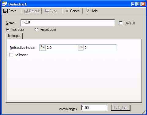
| 4 | Define material in Profile Designer Perform the following sub-steps to define the material that will be used in the example project. (1) In the directory under OptiFDTD_Designer1, Materials folder, right-click the Dielectric folder. A context menu appears. Figure 6: Context Menu (2) Select New. The Dielectric dialog box appears. |
Figure 7: Dielectric dialog box
| (3) Type the following information Name: n=2.0 refractive index (isotropic)(Re): 2.0(4) To save the material, click Store. Material n=2.0 will be listed in the Dielectric folder. (5) Repeat above sub steps (1) – (4) to define second material as (6) Repeat above sub steps (1) – (4) to define third material as (7) Air material is the OptiFDTD default material that will be always exist in the material folder. If Air material does not appear in the material folder list, please follow the step (1) – (4) to define this Air material: Note: (2) You can also select one defined material from the material folder list and drag it into corresponding other material folder in Master folder or other project folder (when you open more projects) |
|
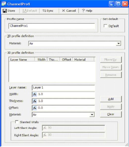
| 5 | Define Channel profile Channel profile is a waveguide cross section that may contain single or multiple rectangular shapes. (1) In the directory under OptiFDTD_Designer1, under the Profiles folder, right click the Channel folder. A context menu appears. (2) Select New. The Channel Profile dialog box appears. |
Figure 8: Channel Profile dialog box
| (3) Type the following Profile name: ChannelPro1.
(4) To define the 2D profile, in the Material list under 2D profile definition, (a)2D Profile will be used for 2D simulations. (b)To define a 3D channel profile, under 3D profile definition: (a)Type the following information: (b)In the Material list, select n=3.0 (c)Click Add. (d)Repeat above step (a)-(c) to add another layer that has the (e)To save the defined channel profile, click Store, ChannelPro1 will Note: |
Figure 9: Two layer channel profile
| (b) Each layer’s dimension is a ratio value. The waveguide’s real dimensions will be set in the waveguide properties dialog box in the layout window.
(c) “Offset” can make the layers shift along the horizontal direction. |
|
| 6 | Define fiber profile
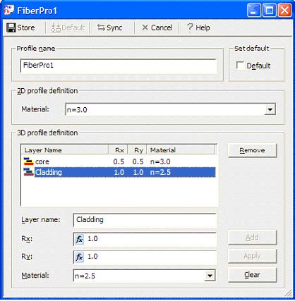
Fiber profile is a waveguide cross section that may contain single or multiple circular or elliptical shapes. (1) In the directory under OptiFDTD_Designer1, under the Profiles folder, right click the Fiber folder. A context menu appears. (2) Select New. The Fiber Profile dialog box appears. (3) Type the following Profile name: FiberPro1. (4) To define the 2D fiber profile, in the Material list under 2D profile definition, select N=3.0. (5) To define the 3D fiber profile, under 3D profile definition: (a)Type the following information: Layer name: Core Rx: 0.5(x-directional radius) Ry: 0.5(y-directional radius) (b)In the Material list, select n=3.0 (c)Click Add. (d)Repeat above step (a)-(c) to add another layer that has the following properties. Layer name: Cladding Rx: 1.0 Ry: 1.0 Material: n=2.5 (e)To save the defined channel profile, click Store, FiberPro1 will be listed under the Fiber Profile folder. |
Figure 10: Two layers fiber profile
Note:
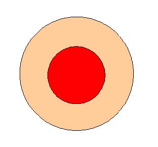
(a) Now we have created a fiber waveguide cross section as shown in Figure 11.
Figure 11: Sketch for Two Layers fiber profile
| (b) The Input dimension is a ratio value. The real fiber waveguide dimension can be re-set in the layout window. |
The material and waveguide cross-sections have now been defined. We can either
leave the Profile designer window open or close it. In the next step we return to the
initial properties dialog box to finish the layout dimension setting.
| 7 | Set initial simulation domain properties
(1) In the Initial Properties dialog Box, click Default Waveguide button. (a) In the Width input box, specify the initial waveguide width as 1.5µm. This is the waveguide width default setting, i.e. when you draw a waveguide in the layout window; the drawn waveguide will has this default width. (b) From the Profile list, Select ChannelPro1 as the default waveguide profile. When you draw a waveguide direction, this channel profile will be linked to your drawn waveguide (2) In the Initial Properties dialog box, click Wafer Dimension button. (a) Input 8.0 (µm) in the Length input box (b) Input 6.0 (µm) in the Width input box Note: (a) In OptiFDTD, we refer to the whole simulation domain as the wafer (b) Length direction is designated as z-direction. The z-directional coordinates for the layout will be from 0 µm to 8 µm for the current setting (c) Width direction is designated as x-direction. The x-directional coordinates for the layout will be from -3 µm to 3 µm for the current setting (3) In the Initial Properties dialog box , Click 3D Wafer Properties (a) In the Substrate area, input the following information Material: n=2; thickness: 3 (µm) (b) In the Cladding area, input the following information Material: Air; thickness: 3 (µm) Note: (a) 3D Wafer Properties control the y direction simulation domain properties. By default, Optiwave automatically sets the wafer with two layers in y-direction. One layer is named “Substrate”, and another layer is named “Cladding”. (b) Interface between substrate and cladding layer will be the y=0 plane. The Substrate thickness can be set as zero to make the whole simulation domain as one background material, later in the layout window, user can fill in other waveguide shapes with different materials. (c) For the current setting, the extent of the y-coordinates for the layout will be from -3 µm to +3um. i.e, from y=-3 µm to y=0 µm, it is the substrate layer with material as n=2, and from 0 µm to 3 µm, it is the cladding layer- Air. (4) In the Initial Properties dialog box , Click 2D Wafer Properties. In the Wafer Refractive Index region set, the material as Air. This step will be set the background material for 2D layout. |
The Initial Properties settings have now been completed. The user can always modify these settings by selecting Wafer Properties or Profile and Material in the edit menu of the OptiFDTD Designer.
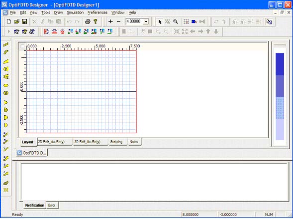
| 8 | Click OK in the Initial Properties Dialog box, OptiFDTD Designer appears. |
Figure 12: OptiFDTD layout Designer
| Note:
(1) OptiFDTD Designer window is the xz– plane view of your layout. (2) For the first time user, we recommend that all the shortcut toolbars be made visible. Also for your convenience the waveguide shape shortcut toolbar can be moved to the left side of the layout window. (3) Click shortcut toolbar “+” or “-” to zoom in or zoom out the layout window. |
|
| 9 | Draw the channel waveguide in the layout window
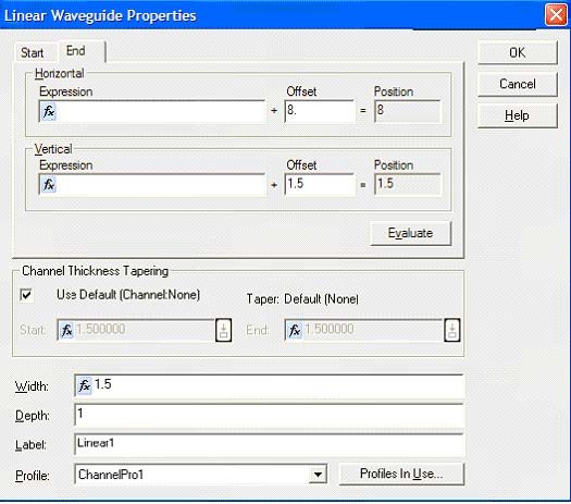
(1) From the Draw menu, select Linear Waveguide. (2) In the layout window, drag the linear waveguide from the start point to the end point. A linear waveguide appears in the layout window. Note: After the Linear Waveguide is drawn in the layout, you must release the Linear Waveguide selection by clicking the arrow button (3) To adjust the position and the shape of the waveguide, in the layout window, double-click the Linear Waveguide. The Linear Waveguide Properties dialog box appears. |
Figure 13: Channel waveguide Properties.
|
(4) Click the Start tab and type the following values Horizontal offset (μm): 0 Vertical offset (μm): 1.5 (5) Click the End tab and type the following values: Horizontal offset (μm): 8.0 Vertical offset (μm): 1.5 Note: (a) Here the Start and End tab control the waveguide x and z coordinates. (b) Horizontal direction is z-direction; Vertical direction is x-direction. (c) In OptiFDTD, all the input boxes marked “fx” can accept variable and expression input. Click Evaluate to see the final value of the expression. (6) Input 1.5 (μm) In the Width box. This is the channel waveguide Width (7) Input 1 (μm) In the Depth box. Depth is the channel waveguide y-direction position. It is the distance from the channel waveguide bottom to the y- coordinate origin. (8) Input Linear1 in the Label box. This is the object name (9) Input ChannelPro1 in the Profile box. This will link the linear waveguide trends with the defined channel profile. (10)Click OK to finish the Channel waveguide setting. Note: (a) In summary, the values for Start Horizontal, Start Vertical, and Depth control the waveguide start point coordinates (1.5, 1.0, 0.0) μm. The values for End Horizontal, End Vertical, and Depth control the waveguide end point coordinates (1.5, 1.0, 8.0) μm. The width and thickness controls the waveguide dimension. (b) If the user wants to set the waveguide thickness ( y-direction thickness), please unselect “Use Default” checkbox under the Channel Thickness Tapering region. The user can then put a start position thickness and an end position thickness. If Use Default checkbox is select, then the waveguide thickness will be the total thickness that is defined in the profile designer. |
|
| 10 | Draw the Fiber waveguide in the layout window
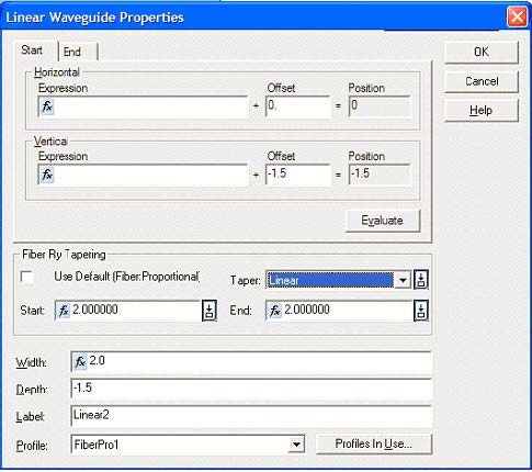
(1) From the Draw menu, select Linear Waveguide. (2) In the layout window, drag the linear waveguide from the start point to the end point. A linear waveguide appears in the layout window. Release the Draw mode by select the select toolbar (3) To adjust the position and the shape of fiber waveguide, in the layout window, double-click the Linear Waveguide. The Linear Waveguide Properties dialog box appears (4) In the Linear Waveguide Properties dialog box, Select FiberPro1 as the profile from the Profile list box. |
Figure 14: Fiber waveguide properties
|
(5) Click the Start tab and insert the following values Horizontal offset (μm): 0 Vertical offset (μm): –1.5 (6) Click the End tab and type the following values: Horizontal offset (μm): 8.0 Vertical offset (μm): -1.5 (7) In the Fiber Diameter Tapering panel, unselect User Default, select Linear in the Taper list box. Set the Start and End values as 2.0 ( the Fiber’s thickness in the y direction) (8) Input the value 2.0 (μm) in the Width box ( the Fiber’s Width in the x-direction) (9) Input the value -1.5 (μm) in the Depth box (the Fiber’s center position in the y direction). (10) Input Linear2 as the Label name. (11) Click OK to finish the Fiber waveguide setting |
Now the sample layout has been created. Please review the following for further
understanding of the layout concept.
Note:
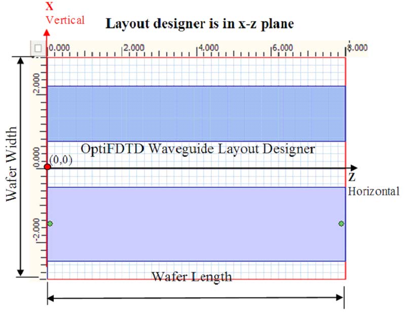
(a) Please note that the OptiFDTD designer environment is a 2D plane for xz
view as shown in Figure 15. Each object may have a different depth
reference to y-direction origin, but the OptiFDTD designer will show all
these objects in this x-z plane top view as shown in figure 15.
Figure 15: OptiFDTD designer for the example layout.
| (b) Figure 16 is the sketch for the OptiFDTD Designer concept for the layout example. |
Figure 16: Sketch for the designed layout
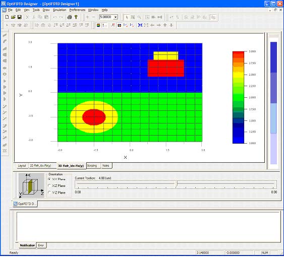
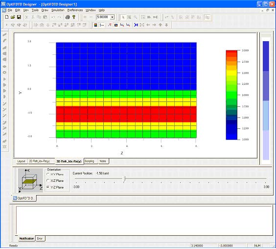
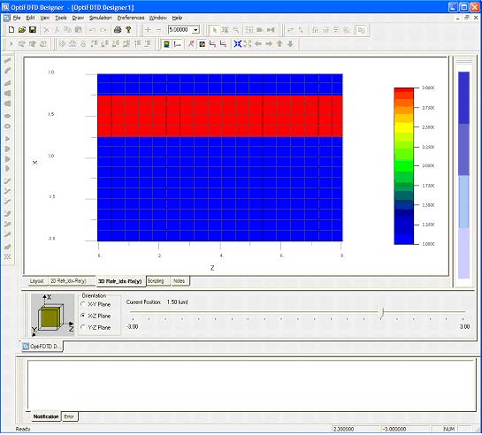
| (c) OptiFDTD designer works only in the x-z plane, but a slice viewer is provided for you to observe the refractive index distribution in any slice in xy plane, yz palne and xz plane. To do this, Please set and input plane first, and Click 3D_Refr_Idx_Re(y) button that is under the layout window. You can specify the slice position and orientation to view to layout See Figure 17 (a)-(c).
Note: The refractive index image resolution is determined by the OptiFDTD simulation mesh size. Click Simulation Parameters in the Simulation menu to re-set the mesh size. (d) To modify the material or the simulation domain. Please click “ Profile and Material “ or the Wafer Properties to open the corresponding interface. |
Figure 17: (a) Refractive indes distribution in xy plane at z=4.00μm
Figure 18: (b) Refractive index distribution in yz plane at x=-1.5μm
Figure 19: (C) Refractive index distribution in xz plane at y=1.5μm


