| Step | Action |
| 1 | Open OptiFDTD Waveguide layout Designer. From the Start menu, select Programs ->Optiwave Software ->OptiFDTD->Waveguide Layout Designer. OptiFDTD_Designer. |
| 2 | Create a new project. From the OptiFDTD_Designer File menu, select New.
The Initial Properties dialog box appears. |
| 3 | Define the material(s) and waveguide profile(s) that will be used in the project. Click the Profiles and Materials button in the Initial Properties dialog. The Profile Designer OptiFDTD opens. At any time, you can open the Profile Designer from the “Edit->Profiles and Materials…” menu of the Layout Designer or from the Start menu, to make any required modifications to the defined materials and profiles.
a. In the directory under OptiFDTD_Designer1 of Profile Designer OptiFDTD, under Materials folder, right-click the Dielectric folder. A context menu appears. Select New, the Dielectric dialog box appears. By default the isotropic material is selected. Type the following information • Name: n=3.3 • Refractive index (Re): 3.3 • Refractive index (Im): 0.0 • Click Store to save this material. Material n=3.3 will be listed under the Dielectric folder b. In the directory under OptiFDTD_Designer1, under the Profiles folder, right click the Channel folder. A context menu appears. Select New. The Channel Profile dialog box appears.Type the following: • Profile name: Channel_2D_n=3.3 • Under 2D profile definition: Select Material n=3.3 • To save the channel profile, click Store. Channel_2D_n=3.3 appears in the Channel folder. This sample just used 2D simulation. It is not necessary to define the 3D profile. After the material and profile are defined, we can return to the initial simulation settings. Note: • After materials and profiles are created, we can come back to the initial properties dialog box; the profile designer can be either left as open or closed. • By clicking Profile and Material under the edit menu of the layout designer, the profile designer can be re-opened at any time to edit/add new material and profile |
| 4 | Type the following information in each corresponding area in the Initial Properties dialog box.
Default Waveguide: Width (um):0.5 Profile:Channel_2D_n=3.3 2D wafer Properties: Wafer refractive index: Material: Air. This is the background material Wafer Dimensions: Length (µm): 2+36*cell_length+2 Width (µm): 3.0 • Wafer dimension is the simulation domain size. Length is the z-direction size. Width is the x-direction size. • In OptiFDTD, the input box marked fx allows user to type the formula and variable. When a variable is being used for the first time in the input box, the software will guide the user to the Edit Parameters dialog box to define this parameter. • In this layout, we set input and output waveguide length as 2.0 and grating length is 36*cell_length. The total simulation domain length is “2+36*cell_length+2”. The variable “cell_length” means the length for each grating period. Later we will define it as cell_length=length01+ length02. |
| 5 | Click OK in Initial Properties Dialog box.
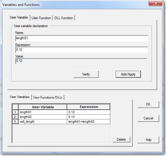
• In General, if no variables are being used in the initial properties dialog box, clicking OK will guide the user to the layout window. • Because we used the variable “cell_length” in the initial settings before we declared it, the software will present an error message: “Error: Unknown variable in the Wafer Length. Do you want to define 2+cell_length+2?”. Click “Yes” to define the variable. “Variable and Functions” dialog box appears (refer to figure 2). |
| 6 | Define variable in the Variable and Functions dialog box
a. In the User variable declaration region, do the following. • Name: length01 • Expression: 0.12 • Click “Verify” button to check the value. • Click “Add/Apply”button to make this variable in the list. b. Repeat above step to define another variable “length02”. • Name: length02 • Expression: 0.13; c. Repeat above step to define the third variable “cell_length”. • Name: cell_length • Expression: length01+length02 d. Click OK button to finish the variable declaration, OptiFDTD Designer window appears. • In OptiFDTD designer window, user can always click “ Edit Parameters” to declare/edit/delete the variables. |
Figure 2: Variable and Function
Note:
• Your shortcut Toolbars may not all appear in the window. You can change it from the “View->Toolbars” menu option.
• Click “+” (zoom) toolbar button to enlarge the layout window
| 7 | Draw the input waveguide in the layout window
• From the Draw menu, select Linear Waveguide, or select the Linear Waveguide shortcut toolbar. • In the layout window, drag the linear waveguide from the start point to the end point. A linear waveguide appears in the layout window. • Change the mouse drawing tool by selecting the arrow shortcut icon on the toolbar. • To adjust the position and the shape of the waveguide, in the layout window, double-click the Linear Waveguide. The Linear Waveguide Properties dialog box appears. • Click the Start tab and type the following values: Horizontal offset (um): 0.0 (Start point for z-direction) Vertical offset (um): 0.0 (Start point for x-direction) • Click the end tab and type the following values: Horizontal offset (um): 2.0 (end point for z-direction) Vertical offset (um): 0.0 (end point for x-direction) • Width(um): 0.5 • Label: Linear1 • Profile: Channel_2D_n=3.3 • Click OK to finish the input waveguide setting |
| 8 | Draw the output waveguide in the layout window. Repeat step 7 to create the output waveguide by using the following information:
Start Horizontal Expression (um): 2+36*cell_length Start Horizontal Offset (um): 0.0 Start Vertical Offset (um): 0.0 End Horizontal Expression(um): 2+36*cell_length+2 End Horizontal Offset (um): 0.0 End Vertical offset (um): 0.0 Width(um): 0.5 Label: Linear2 Profile: Channel_2D_n=3.3 |
Figure 3: Crystal Lattice properties
| 9 | Draw the Grating Layout. There are two ways to define the periodic structure:
one is to use the VB script (please refer to tutorial lesson 15 part 1), another one is to use the PBG editor. The following are the steps for using the PBG editor to define this periodic grating layout. a. From the Draw menu, select PBG Crystal Structure (or select the shortcut toolbar for PBG Crystal Structure). b. In the layout window, drag the cursor in a designated starting point and release it to create the PBG area. The PBG Crystal Structure appears in the layout window. It is a rectangular line with a green dot as original point. (Change the mouse drawing tool by selecting the arrow shortcut icon on the toolbar) c. To edit periodic grating, double-click on this rectangular object in the layout. The Crystal Lattice Properties dialog box appears, as shown in Figure 3. d. In Origin, Offset, type/select the following: Horizontal: 2.0 (grating start position for z-direction) Vertical: 0 (grating start position for x-direction) e. Depth: 0. — (y-direction original position, not used in this layout) Azimuth: 0.0 (rotation angle, not used in this layout) f. Lattice Properties (i.e. the periodic relation): Type: 2D Rectangular Fill: Block Note: Periodic relation is controlled by three Vectors: A, B, C g. Lattice Dimension (i.e. Periodic distance and number of periodic cells): Scale: cell_length Note: • Clicking the OK button in the Crystal Lattice Properties interface in this step will return you to the layout window. Now the 36 grating cells are being generated. But no waveguide is filled in each cell. Double clicking on this periodic region will activate the Crystal Lattice Properties interface again to do the further editing h. Define waveguides for each periodic cell. Objects in each periodic cell will be called Atom Waveguides. • In Atom Waveguide in Unit Cell, Add New, select Linear Waveguide from the drop-down menu and click New. The Linear Waveguide Properties dialog box appears • Type the following Start Horizontal Offset: 0.0 Start Vertical offset: 0.0 End Horizontal Expression: length01 End Horizontal Offset 0.0 End Vertical offset: 0.0 Width 0.7 Depth 0.0 Label Atom Profile Channel_2D_n=3.3 Note: Atom waveguide position take each cells original position as reference. • Click OK to finish the first atom waveguide settings. • Repeat the above action to define the second atom waveguide with following information: Start Horizontal Expression: length01 Start Vertical offset: 0.0 Start Horizontal offset: 0.0 End Horizontal Expression: cell_length Start Horizontal Offset (um): 0.0 Start Vertical offset: 0.0 Width 0.5 Depth 0.0 Label Atom1 Profile Channel_2D_n=3.3 |
Click OK in the Crystal Lattice properties dialog box to finish/accept the grating layout creation. Now the whole layout will be generated. (refer to Figure 4)
Figure 4: Grating layout.
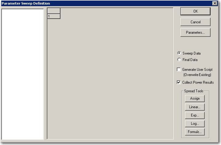
Figure 5: Parameter Sweep Definition


