OptiFDTD provides two dimension nonlinearity and multiple input wave simulations, thereby enabling you to simulate the Four Wave Mixing (FWM) effect. The following lesson outlines how OptiFDTD performs a FWM simulation.
To create the Four Wave Mixing layout, perform the following procedures.
Designing a four-wave mixing layout
To design the four-wave mixing materials, perform the following procedures.
| Step | Action |
| 1 | Start Waveguide Layout Designer. |
| 2 | To create a new project, select File > New.
The Initial Properties dialog box appears. |
| 3 | Click Profiles and Materials.
The Profile Designer window appears. |
| 4 | Under the Materials folder, right-click the Dielectric folder and select New.
A new FDTDDielectric1 material dialog box appears. |
| 5 | Select/type the following information:
Name: FDTD_1.65 Const Ref. Idx N Re: 1.65 |
| 6 | To save the material, click Store.
FDTD_1.65 appears in the Dielectric folder in the directory and in the dialog box title bar. |
| 7 | Under the Materials folder, right-click the FDTD-Nonlinear folder and select New.
A new FDTDNonlinear1 material dialog box appears. |
| 8 | Select Kerr.
The Kerr tab appears in the dialog box. |
| 9 | Select/type the following:
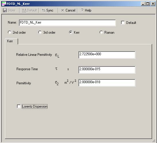
Name: FDTD_NL_Kerr Relative Linear Permittivity: 2.7225 Response Time: 2.0e-15 Permittivity: 2.0e-18 |
| 10 | To save the material, click Store. |
Figure 19: FDTD_NL_Kerr material
To define the channel profile, perform the following procedure.
| Step | Action |
| 1 | Under the Profiles folder, right-click the Channel folder and select New.
The ChannelPro1 dialog box appears. |
| 2 | Create the following channel profile:
Profile name: NL_Kerr 2D profile definition Material: FDTD_NL_Kerr |
| 3 | Click Store. |
| 4 | Create a second profile:
Profile name: Linear_WG 2D profile definition Material: FDTD_1.65 |
| 5 | Click Store. |
| 6 | Close the Profile Designer. |
To define the wafer and waveguide properties, perform the following procedure.
| Step | Action |
| 1 | In the Initial Properties dialog box, , type/select the following:
Waveguide Properties Width [μm]: 1.0 Profile: NL_Kerr Wafer Dimensions Length [μm]: 15.0 Width [μm]: 10.0 2D Wafer Properties Material: Air |
| 2 | Click OK.
The Initial Properties dialog box closes and the layout window appears. |
To create the waveguide, perform the following procedure.
| Step | Action |
| 1 | From the Draw menu, select Linear Waveguide. |
| 2 | In the layout window, drag the linear waveguide from the start point to the end point.
A linear waveguide appears in the layout window. Note: Release the Linear Waveguide selection tool by clicking the Select tool after the Linear Waveguide is drawn in the layout. |
| 3 | To adjust the position and the shape of the waveguide, in the layout window, double-click the Linear Waveguide.
The Linear Waveguide Properties dialog box appears. |
| 4 | Click the Start tab. |
| 5 | Under Offset, type the following values:
Horizontal: 4.0 Vertical: 0 |
| 6 | Click the End tab |
| 7 | Under Offset, type the following values:
Horizontal (µm): 13.00 Vertical (µm): 0.0 |
| 8 | In Channel Thickness Tapering, select Use Default (Channel:None). |
| 9 | Type/select the following:
Width (µm): 8.0 Depth (µm): 0.0 Label: linear4 Profile: NL_Kerr |
| 10 | Click OK. |
| 11 | Repeat steps [1] through [3] to create three input linear waveguides in the layout.
Note: The input waveguide is used to input three different wavelength waves into the nonlinear material. |
Input Waveguide 1 properties:
| Step | Action |
| 1 | In Start > Offset, type the following values.
Horizontal: 0 Vertical: 0 |
| 2 | In End > Offset, type the following values:
Horizontal: 4 Vertical: 0 |
| 3 | In Channel Thickness Tapering, select Use Default (Channel:None). |
| 4 | Type/select the following:
Width (µm): 1.0 Label: linear1 Depth (µm): 0.0 Profile: Linear_WG |
| 5 | Click OK. |
Input Waveguide 2 properties:
| Step | Action |
| 1 | In Start > Offset, type the following values.
Horizontal: 0 Vertical: 1.2 |
| 2 | In End > Offset, type the following values:
Horizontal: 4 Vertical: 1.2 |
| 3 | In Channel Thickness Tapering, select Use Default (Channel:None). |
| 4 | Type/select the following:
Width (µm): 1.0 Depth (µm): 0.0 Label: linear2 Profile: Linear_WG |
| 5 | Click OK. |
Input Waveguide 3 properties:
| Step | Action |
| 1 | In Start > Offset, type the following values.
Horizontal: 0 Vertical: -1.2 |
| 2 | In End > Offset, type the following values:
Horizontal: 4 Vertical: -1.2 |
| 3 | In Channel Thickness Tapering, select Use Default (Channel:None). |
| 4 | Type/select the following:
Width (µm): 1.0 Depth (µm): 0.0 Label: linear3 Profile: Linear_WG |
| 5 | Click OK. |
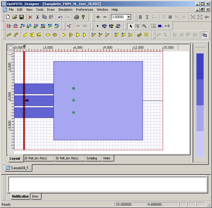
Figure 20: Input waveguides
Setting the input wave
| Step | Action |
| 1 | From the Draw menu, select Vertical Input Plane. |
| 2 | To insert the input plane, click in the layout window where you want it placed.
The input plane appears in the layout. |
| 3 | To edit the input plane, double-click on the input plane in the layout.
The Input Plane Properties dialog box appears. |
| 4 | On the General tab, type/select the following:
Continuous Wave Wavelength [μm]: 1.4 Input Field Transverse: Modal Plane Geometry: Z Position [μm]: 1.0 |
| 5 | On the 2D Transverse tab, click Find Modes.
The Mode Solver 2D dialog box appears. |
| 6 | On the Waveguides tab, select Linear1. |
| 7 | Click Calculate Mode.
The Modes tab is activated. |
| 8 | On the Modes tab, select the mode. |
| 9 | Click Apply Data.
The Mode Solver 2D closes. |
| 10 | On the 2D Transverse tab, select the Amplitude radio button and type the following:
Amplitude [V/m]: 2.0e09 |
| 11 | Click OK.
The Input Field Properties dialog box closes. |
| 12 | Repeat steps [1] through [10] to create a second vertical input plane with the following data: |
Vertical Input Plane 2 properties:
| Step | Action |
| 1 | In the Input Field Properties dialog box, select/type the following:
Continuous Wave Wavelength [μm]: 1.55 |
| 2 | On the General tab, type/select the following:
Input Field Transverse: Modal Plane Geometry: Z Position [μm]: 1.0 |
| 3 | Click Find Modes.
The Mode Solver 2D dialog box appears. |
| 4 | On the Waveguides tab, select Linear2. |
| 5 | Click Calculate Mode.
The Modes tab is activated. |
| 6 | On the Modes tab, select the mode. |
| 7 | Click Apply Data.
The Mode Solver 2D closes. |
| 8 | On the 2D Transverse tab, select the Amplitude radio button and type the following:
Amplitude [V/m]: 2.0e09 |
| 9 | Click OK.
The Input Field Properties dialog box closes. |
Vertical Input Plane 3 properties:
| Step | Action |
| 1 | In the Input Field Properties dialog box, select/type the following:
Continuous Wave Wavelength [μm]: 1.60 |
| 2 | On the General tab, type/select the following:
Input Field Transverse: Modal Plane Geometry: Z Position [μm]: 1.0 |
| 3 | Click Find Modes.
The Mode Solver 2D dialog box appears. |
| 4 | On the Waveguides tab, select Linear3. |
| 5 | Click Calculate Mode.
The Modes tab is activated. |
| 6 | On the Modes tab, select the mode. |
| 7 | Click Apply Data.
The Mode Solver 2D closes. |
| 8 | On the 2D Transverse tab, select the Amplitude radio button and type the following:
Amplitude [V/m]: 2.0e09 |
| 9 | Click OK.
The Input Field Properties dialog box closes. |
Setting up the Observation Point
| Step | Action |
| 1 | From the Draw menu, select Observation Point. |
| 2 | Place the Observation Point in the desired position in the layout. |
| 3 | Double-click the observation point.
The Observation Properties — Point dialog box appears. |
| 4 | On the General tab:
In Center, Offset, type/select the following: Horizontal: 6.0μm Vertical: 0.0μm Center depth: 0.0 μm Label: Observation Point1 |
| 5 | On the Data Components tab, ensure that 2D TE: Ey is selected (default). |
| 6 | Click OK.
The Observation Properties — Point dialog box closes. |
| 7 | Repeat steps 1 to 5 and create another Observation Point with the following information. |
| 8 | On the General tab:
In Center, Offset, type/select the following: Horizontal: 6.0μm Vertical: 1.2μm Center depth: 0.0 μm Label: Observation Point2 Click OK. |
| 9 | Repeat steps 1 to 5 and create another Observation Point with the following information. |
| 10 | On the General tab:
In Center, Offset, type/select the following: Horizontal: 6.0μm Vertical: -1.2μm Center depth: 0.0 μm Label: Observation Point3 |
| 11 | On the Data Components tab, ensure that 2D TE: Ey is selected (default). |
| 12 | Click OK. |
Setting the 2D simulation parameters
| Step | Action |
| 1 | From the Simulation menu, select 2D Simulation Parameters.
The Simulation Parameters dialog box appears. |
| 2 | Type/select the following information:
Polarization: TE Mesh Delta X [μm]: 0.1 Mesh Delta Y [μm]: 0.1 |
| 3 | Click Advanced….
The Boundary Conditions dialog box appears. |
| 4 | Type/select the following information:
-X: Anisotropic PML +X: Anisotropic PML -Z: Anisotropic PML +Z: Anisotropic PML Anisotropic PML Calculation Parameters Number of Anisotropic PML Layers: 10 Theoretical Reflection Coefficient: 1.0e-12 Real Anisotropic PML Tensor Parameters: 5.0 Power of Grading Polynomial: 3.5 |
| 5 | In Time Parameters, click Calculate.
The default time step size is calculated. |
| 6 | Select Run for 3000 Time Steps (Results Finalized). |
| 7 | Select Key Input Information: Input Plane1 and wavelength:1.4.
Note: The input plane’s center wavelength is used for DFT calculations. |
| 8 | Click OK to close the Simulation Parameters dialog box without running the simulation, or click Run to start the OptiFDTD Simulator.
Note: Save your layout before starting the simulation. |
Observing the simulation results
Key things to observe:
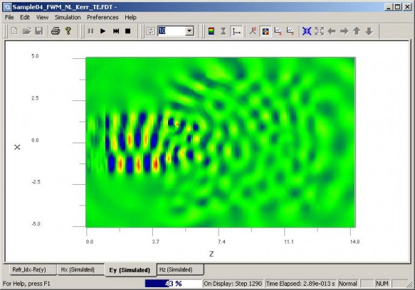
- wave propagation pattern in time domain (see Figure 21)
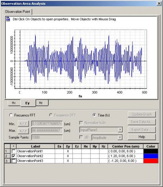
- field response in time domain and frequency domain for observation point (select View > Observation Point to see the dynamic time domain and frequency domain response (see Figure 22).
Figure 21: OptiFDTD Simulator—wave propagation pattern in time domain
Figure 22: OptiFDTD Simulator—time domain and frequency domain for observation point


