OptiFDTD provides two types of Dispersive material simulations:
- Multiple Resonant Lorentz
- Drude
The Drude model is supposed to be used for the Noble Metal and Surface Plasma in optical band.
Note: It is recommended that you read the section in the Technical Background describing the Drude model equation. OptiFDTD also provides a sample for a Drude model simulation. The following explanation uses this sample file as an example.
The corresponding layout file is available in the sample folder of OptiFDTD:
Sample15_2D_TE_Drude_Model_Emitting_Diode.FDT.
The corresponding results file is available on the OptiFDTD setup CD:
Sample15_2D_TE_Drude_Model_Emitting_Diode.FDA.
Creating a project with Drude material
| Step | Action |
| 1 | Start Waveguide Layout Designer. |
| 2 | To create a new project, from the File menu, select New.
The Initial Properties dialog box appears. |
| 3 | Click the Profiles And Materials.
The Profile Designer appears. |
| 4 | In the directory under OptiFDTD_Designer1 of the Profile Designer, under the Materials folder, right-click the FDTD-Dispersive folder, and select New. The FDTDDielectric1 material definition dialog box appears. |
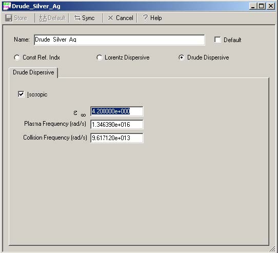
| 5 | In the FDTD Dielectric1 material definition dialog box, select Drude Dispersive.
The Dispersive Material Definition dialog box appears (see Figure 1). |
Figure 1: Dispersive Material Definition dialog box
| 6 | In the Drude Material Definition dialog box, define the following parameters:
Name: Drude_Silver_Ag ε∞ (F/m): 1.999 Plasma Frequency: 1.346390e+016 Collision Frequency: 9.617120e+013 |
| 7 | Click Store to save the material. |
| 8 | In the directory under OptiFDTD_Designer1 of the Profile Designer, under the Materials folder, right-click the Dielectric folder, and select New.
The Dielectric1 material definition dialog box appears. |
| 9 | Design a linear material with refractive index equal to 1.414 and Material name Dielectricn=1.414. |
| 10 | Click Store. |
| 11 | In the directory under OptiFDTD_Designer1, Profile folder, right-click the Channel folder, and select New.
The ChannelPro1 dialog box appears. |
| 12 | In the ChannelPro1 dialog box, set Profile Name to Ag and 2D Profile Material to Drude_Silver_Ag. |
| 13 | Save the profile. |
| 14 | Design another 2D channel profile with the name Core and material Dielectricn=1.414. |
| 15 | Click Store. |
| 16 | Close the Profile Designer. |
Designing the waveguides
| Step | Action |
| 1 | In the Initial Properties dialog box, set the following parameters:
Waveguide Properties Width: 0.12μm Profile: Core Wafer dimension Length: 1.8μm Width: 1.4μm 2D Wafer Material: Air |
| 2 | Click OK to start the Layout Designer.
The OptiFDTD designer window appears. |
| 3 | From the Draw menu, select Linear Waveguide. |
| 4 | Draw the waveguide in the layout at desired the position.
The waveguide appears in the layout. Note: Click the Select tool after drawing the waveguide. |
| 5 | Double click the waveguide to edit the waveguide position and properties.
The Linear Waveguide properties dialog box appears. |
| 6 | Set the following parameters:
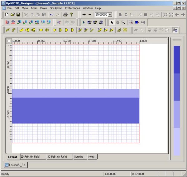
Waveguide start position Horizontal: 0 Vertical: 0 Waveguide end position Horizontal: 1.8 Vertical: 0 Select Use Default checkbox. Width: 0.12 Depth: 0.0 Profile: Core |
| 7 | Design another linear waveguide with following properties:
Waveguide start position Horizontal: 0 Vertical: –0.24 Waveguide end position Horizontal: 1.8 Vertical: –0.24 Select Use Default checkbox. Start thickness: 1.0 End thickness: 1.0 Width: 0.36 Depth: 0.0 Profile: Ag The two waveguides appear in the layout, the upper one is the linear waveguide, which will guide the wave, and the lower one is the Substrate Silver layer in the emitting diode (see Figure 2). |
Figure 2: Waveguides in the layout
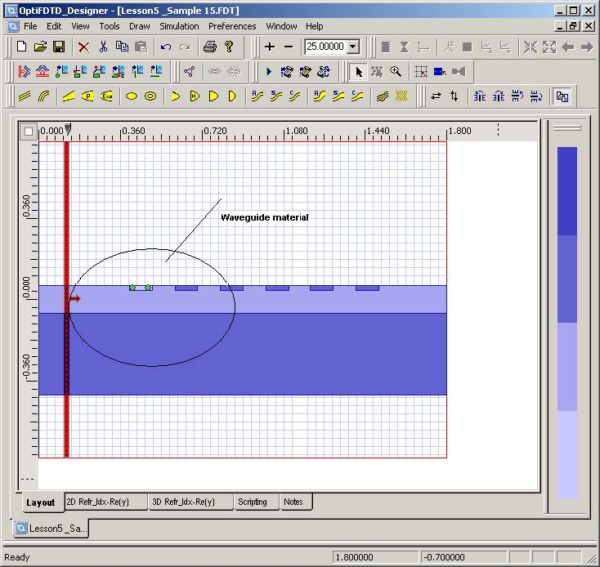
To enhance the Light Fitting, a corrugated surface plasma is deposited in the core. To do this, periodic rectangular linear waveguides are designed following the waveguide design outline in the previous procedure.
Each of the rectangular linear waveguides that make up the corrugated surface plasma has the following common parameters (see Figure 3):
Width: 0.02μm
Depth: 0.0μm
Select Use Default checkbox.
Note: Thickness is only used for 3D layout definitions.
Profile: Ag
Start vertical: 0.05μm
End vertical: 0.05μm
The six Start/End horizontal positions are:
i. 0.4μm/0.5μm
ii. 0.6μm/0.7μm
iii. 0.8μm/0.9μm
iv. 1.0μm/1.1μm
v. 1.2μm/1.3μm
vi. 1.4μm/1.5μm
Figure 3: Waveguide materials
Setting the Input Plane
| Step | Action |
| 1 | From the Draw menu, select Vertical Input Plane. |
| 2 | Insert the Input Plane into the layout at the desired position.
A red line representing the input plane appears in the layout window. |
| 3 | Double-click the Input Plane.
The Input Field Properties dialog box appears. |
| 4 | Select Continuous Wave. |
| 5 | Set the center wavelength to 0.4um. |
| 6 | Click the General tab, and then click Modal. |
| 7 | Click the 2D Transverse tab to start solving the 2D TE fundamental mode for the Core (Waveguide Linear1) waveguide. |
| 8 | Click Calculate Mode button. |
| 9 | On the Modes tab, select Solved Mode. |
| 10 | Click Apply Data. |
| 11 | Return to the Input Field Properties dialog box and click General tab. |
| 12 | Set Plane Geometry Position to 0.125. |
| 13 | Select Positive direction. |
| 14 | Click OK. |
Setting up 2D Simulation parameters
| Step | Action |
| 1 | From the Simulation menu, select 2D Simulation Parameters.
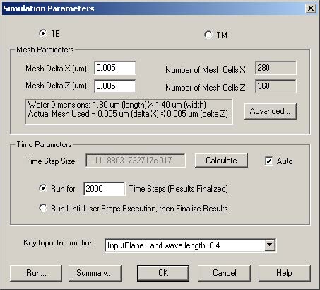
The Simulation Parameters dialog box appears (see Figure 4). |
Figure 4: Simulation Parameters dialog box
| 2 | Click TE. |
| 3 | Set x-direction mesh and z-direction mesh to 0.005. |
| 4 | Click Advanced. |
| 5 | Set the Anisotropic PML boundary condition parameters:
Number of Anisotropic PML layer: 14 Theoretical Reflection Coefficient: 1.0e-12 Real Anisotropic PML Tensor Parameter: 1.0 Power of Grading Polynomial: 3.5 |
| 6 | Click Calculate to get the Time Step Size. |
| 7 | Set Run for 2000 time steps for finalization. |
| 8 | From the Key Input Plane drop-down list, select Input Plane1 and Wavelength to 0.4.
Note: The Key Input Plane’s Center Wavelength will be used for the DFT calculation. |
| 9 | Click OK to close the Simulation Parameters dialog box without running the simulation, or click Run to start the OptiFDTD Simulator. |
Performing the simulation
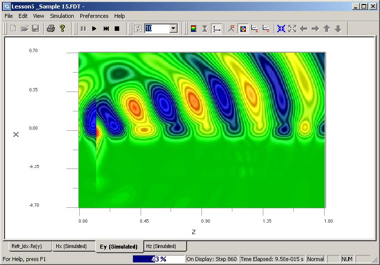
When the Simulator starts, the emitting field can be observed (see Figure 5).
Note: Please use the Rainbow_Banded Palette to view the graph. Right-click on the graph to set the graph control.
Figure 5: OptiFDTD_Simulator
Performing data analysis
With the example used in this lesson, in the Analyzer you can perform the following analysis:
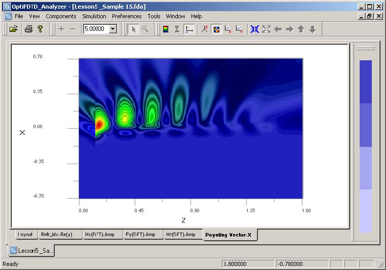
- Observe the Layout, Refractive Index Poynting Vector, field propagation pattern (DFT results) for the Input Wavelength (see Figure 6).
Figure 6: X-direction Poynting Vector
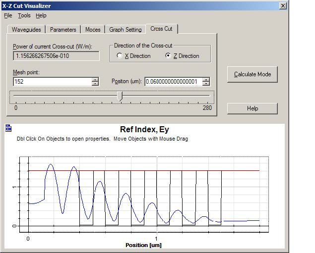
- Select the Cross Cut in the Tools menu to get the Mode Analysis, slice power, and far field transformation. The X-Z Slice viewer appears (see Figure 7).
Figure 7: X-Z Slice viewer


