OptiBPM is a computer-aided design software tool enabling the design of complex optical waveguides, which perform guiding, coupling, switching, splitting, multiplexing, and demultiplexing of optical signals in photonic devices. OptiBPM is based on the Beam Propagation Method (BPM) of simulating the passage of light through any waveguide medium, both isotropic and anisotropic. OptiBPM can observe the near field distribution and examine the radiation and guided field simultaneously. As a result, OptiBPM can improve a design engineer’s productivity, reduce risk, and lower overall costs related to the design of waveguide devices.
Applications
- Design optical splitters, combiners, couplers, multiplexers, and modulators.
- Large-scale optical circuit design capabilities
- Mature AWG design environment
- Model non-symmetrical waveguide structures
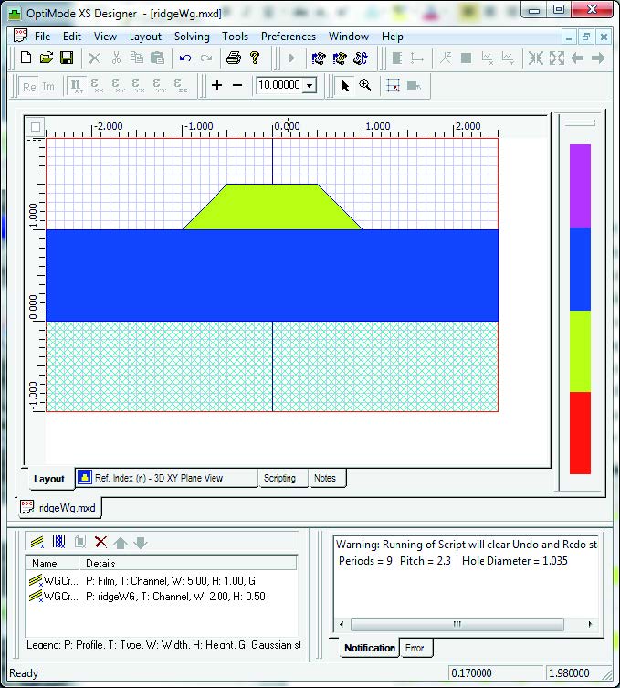
- Channel, rib, or ridge waveguide design
- Buried waveguides
- Waveguides from a diffused process
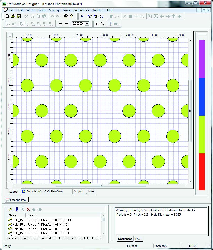
- Sensor structures

KEY FEATURES AND FUNCTIONALITY
Integrated Environment
OptiBPM can combine channel, fiber, and diffused waveguides into a single layout. A simple menu selection allows a layout to be simulated in either 2D or 3D. Integration with OptiSystem delivers continuity in simulation from the waveguide to the system or subsystem level. In addition, complex field data transfer between OptiFDTD and popular ray tracing tools allows OptiBPM designers to incorporate free space optical elements.
Waveguide Shapes
Many waveguide shapes are available, including Linear, Arc, Tapered (Linear, Parabolic, and Exponential), and S-Bend (Arc, Sine, and Cosine). Waveguides are fully parameterized, so waveguide position and all other waveguide properties can be controlled with simple expressions. User-defined waveguides allow arbitrary shapes to be created and used in a layout. These custom
waveguide shapes can be defined in terms of their path or by specifying the upper and lower arms of the waveguide. Any waveguide shape that standard functions of a single variable can describe can be entered.
Waveguides can be created and placed with a mouseclick or VB Script commands. Waveguides can be tapered in width and length in the X-Z plane and height in the Y axis. In addition, waveguides can be tapered in thickness, channel waveguides can be tapered linearly, and fibers can be tapered linearly or proportionately.
Import from AutoCAD DXF and GDSII File Formats
Import and export to and from these standard mask layout formats are supported in OptiBPM. Once you have designed and simulated your waveguide circuit in OptiBPM, you can export the optimized design as a mask for fabrication.
Fiber Vector and LP Mode Solver
Mode solvers based on a mesh can have limitations unacceptable for optical fiber calculations. For example, the magnitude of the fields far from the fiber core can be orders of magnitude smaller than the error made in meshed simulations. However, those small fields can still be significant over long propagation distances. OptiBPM has a multi-layer fiber mode solver that uses a transfer matrix technique for LP and fiber vector modes instead of meshes. As a result, accurate estimation of the field over many orders of magnitude is possible.
Advanced Optimization Algorithms
A good design can be obtained with physical insight and knowledge of fundamental design principles. However, finding the best design usually involves a tedious phase of optimization. OptiBPM has Optimization Algorithms that fully automate this critical step. In addition, OptiBPM uses well-established algorithms such as the Golden Search for one dimension and the Simplex or Direction Set methods for multidimensional searches.
Analysis of Large Scale Optical Circuits
BPM techniques work on a microscopic level (typically, the smallest distance is about 0.1 μm), but photonic circuits, on the other hand, can occupy an entire wafer (scale: 10 cm). Successful analysis needs to combine the basic microscopic techniques with an approach at a more abstract or system level. OptiBPM has the Scattering Data feature, in which the Transfer Matrix of any device can be obtained. Once characterized this way, the device (a subsection of the layout of the entire optical circuit) can be uploaded to OptiSystem. The analysis of the optical circuit as an optical system is very efficient, enabling the design of advanced photonic circuits such as Lattice Filters, Interleavers, Ring-Coupled Resonators, and AWGs.
Electro-Optic Simulation
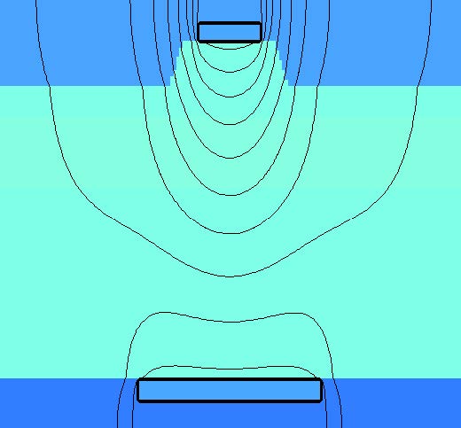
OptiBPM can simulate the linear electro-optic effect (Pockels Effect). You can make electrodes of any shape and add them to the layout. OptiBPM will calculate the static (or radio frequency) electric field in the transverse plane and calculate the optical propagation modified by the electro-optic effect.
No Additional Modules to Purchase
- Includes robust 2D/3D Mode Solvers
- GDSII and DXF output mask formats
- XP/Vista and Windows 7 Compliant
Interface with Popular Design Tools and Measurement Equipment

OptiMode
OptiMode is a complete software suite dedicated to the modal analysis of waveguides, which is the first job in optical component design. A number of numerical algorithms can analyze any waveguide, and many levels of analysis are possible, including scalar, semi-vector, full vector, electric formulation, magnetic formulation, isotropic, and anisotropic. The waveguide design can be parameterized and optimized. Complex waveguides (such as photonic crystals) can be created with VB Scripts written in either OptiBPM or OptiFDTD. Copying profiles and materials (by simple drag-and-drop) between OptiMode, OptiBPM, and OptiFDTD is permitted as they all share the same Profile Designer. Post-processing and review of simulation data are accomplished using OptiMode Analyzer.